
Silicon Nanosponge Particles

a technology of silicon nano-sponge particles and nano-sponge particles, which is applied in the field of porous silicon, can solve the problems of difficult scaling up of this process, many drawbacks and limitations of the process, and the possibility of cracking in the silicon structur

Inactive Publication Date: 2006-11-09
VESTA RES
View PDF23 Cites 72 Cited by
  • Summary
  • Abstract
  • Description
  • Claims
  • Application Information

AI Technical Summary

Benefits of technology

[0008] Silicon nanosponge particles are prepared from a metallurgical grade silicon powder. The metallurgical grade silicon powder has an initial particle size ranging from about 1 micron to about 4 microns. The metallurgical grade silicon powder is treated to yield silicon particles having a particle size ranging from about 0.1 microns to about 40 microns. The silicon particles are separated to isolate the silicon particles having sizes ranging from about 1 micron to about 4.0 microns. The isolated silicon particles are etched to yield silicon nanosponge particles. The silicon nanosponge particles are unique in that each particle comprises a plurality of nanocrystals with pores disposed between the nanocrystals and throughout the entire nanosponge particle. These unique, completely porous silicon nanosponge particles differ from the individual etched particles found in the prior art because porosity is not limited only to the surface of the particle but penetrates throughout the particle and there is no solid core beneath the porous surface. The completely porous or nanosponge structure of each particle enables the silicon nanosponge particles of the present invention to be useful as a carrier material for a broad range of applications such as catalysts and drugs, adsorbents, sensors, explosives, photosensitizers, precursors for high surface area forms of ceramics such as SiC and Si3N4 and as electrodes in fuel cells. The nanosponge material may also be broken down through various milling processes to yield discrete nanocrystal particles useful as intermediates for other applications.

Problems solved by technology

This process has several drawbacks and limitations.
During the processes of drying the porous layer and agitation, the silicon structure is likely to crack.
Next, scale-up of this process is difficult because the yield of porous silicon from the process is limited by the diameter of the silicon wafers.
In addition, there are many challenges in scaling up electrochemical etching processes to large diameter wafers.
Some of these challenges include: the difficulty in achieving a safe and reliable cell design for withstanding extremely corrosive chemicals; making an ohmic contact over the back side of the wafer in order to ensure uniform etching; controlling flow of the electrolyte across the wafer for uniform current density; and the general cost of large diameter silicon wafers.
Thus, the process is limited by the presence of HNO2 at the surface of the silicon sample.
However, in all instances, the resulting silicon nanoparticles must be separated from the remnants of the larger silicon particles and the porosity is limited to a maximum thickness of only 500 nm (0.5 microns).

Method used


Image

  • Silicon Nanosponge Particles
  • Silicon Nanosponge Particles
  • Silicon Nanosponge Particles

Examples


example

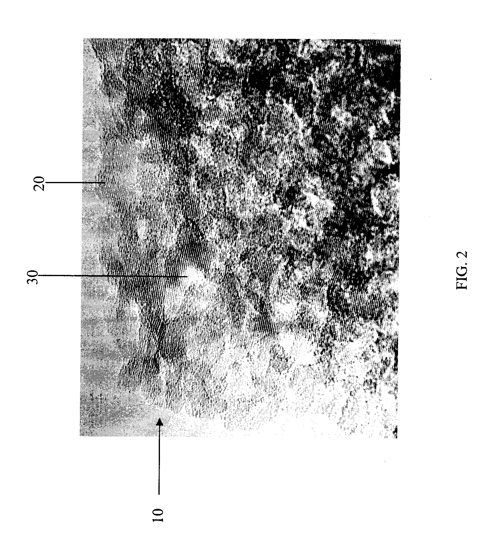
[0033] Silicon nanosponge particles were prepared from 2E, 4E and 4F metallurgical grade silicon powders from Vesta Ceramics, AB in Sweden. The metallurgical grade silicon powders were etched with 750 ml of a 48% HF acid with 1000 ml of water in a propylene bath set at a temperature of 27° C. 100 grams of metallurgical grade silicon powder of the selected grade was added to form a mixture, which was mixed thoroughly. An approximately 25% solution was prepared from a 65% HNO3 reagent. Approximately 400 ml of the 25% HNO3 solution was added in steps. The reaction product was checked for photoluminescence with an ultraviolet light. A bright orange emission indicated the formation of nanocrystals within the silicon particles. The reaction was terminated. The powder was collected and dried under vacuum or in air at 70° C. for 24 hours. The Brunauer-Emmet-Teller (BET) surface area was obtained by nitrogen gas adsorption measurements in a Micromeretics ASAP 2010 gas adsorption analyzer. Sa...


PUM

PropertyMeasurementUnit
Temperatureaaaaaaaaaa

Abstract

Silicon nanosponge particles prepared from a metallurgical grade silicon powder having an initial particle size ranging from about 1 micron to about 4 microns is presented. Each silicon nanosponge particle has a structure comprising a plurality of nanocrystals with pores disposed between the nanocrystals and throughout the entire nanosponge particle.

Description

CROSS-REFERENCE TO RELATED APPLICATIONS [0001] This application claims the benefit of U.S. Provisional Patent Application Serial No. 60 / 678,979, entitled, “Silicon Nanosponge Particles, Articles and Method Relating Thereto,” filed May 9, 2005, which is hereby incorporated by reference in its entirety.FIELD OF THE INVENTION [0002] The present invention is related to porous silicon. In particular, it is related to silicon nanosponge particles prepared from metallurgical grade silicon powder, each particle comprising a plurality of nanocrystals with pores disposed between the nanocrystals and throughout the entire particle. BACKGROUND OF THE INVENTION [0003] The anodization of single crystalline silicon wafers in hydrofluoric acid (HF)-ethanol solutions, results in the formation of pores along certain crystal orientations <100>. This form of silicon is known as porous silicon and is typically formed by immersing a single crystalline wafer in an HF-ethanol electrolyte and applying...

Claims


Application Information

Patent Timeline
IPC IPC(8): C01B33/00
CPCY10T428/2982C01B33/02
Inventor FARRELL, DECLANLIMAYE, SANTOSH Y.SUBRAMANIAN, SHANTHI
Owner VESTA RES
Learn More