Mode-locked semiconductor lasers with quantum-confined active region

a semiconductor laser and active region technology, applied in the field of mode-locked semiconductor lasers with quantum-confined active regions, can solve the problems of increasing the peak power that can be output by the laser, and achieve the effects of reducing the optical power density and accelerating the saturation of the absorber section

Inactive Publication Date: 2006-10-05
INNOLUME ACQUISITION
View PDF99 Cites 23 Cited by
  • Summary
  • Abstract
  • Description
  • Claims
  • Application Information

AI Technical Summary

Benefits of technology

[0007] The present invention overcomes the limitations of the prior art by providing a quantum-confined mode-locked semiconductor laser in which the “mode size” of an absorption region in the laser cavity is increased relative to the mode size of the gain region in the laser cavity. In more detail, the semiconductor laser includes a laser cavity with an optical path. A gain section and an absorber section are located along the optical path and produce loss modulation leading to the mode-locked behavior. The gain section and / or the absorber section contain a quantum-confined active region. The mode volume of the absorber section is increased (e.g., in length and / or cross-sectional area), thus reducing the optical power density in the absorber section. This, in turn, delays saturation of the absorber section until higher optical powers, thus increasing the peak power that can be output by the laser.

Problems solved by technology

This, in turn, delays saturation of the absorber section until higher optical powers, thus increasing the peak power that can be output by the laser.

Method used


Image

  • Mode-locked semiconductor lasers with quantum-confined active region
  • Mode-locked semiconductor lasers with quantum-confined active region
  • Mode-locked semiconductor lasers with quantum-confined active region

Examples


Embodiment Construction

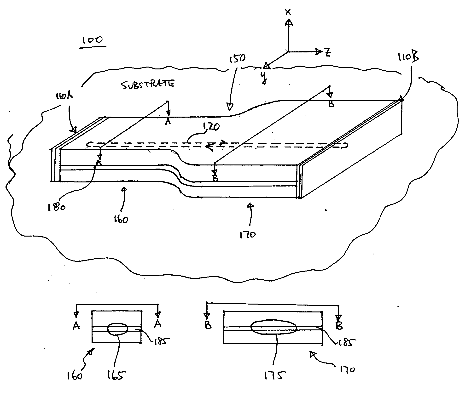
[0021]FIG. 1 is a diagram of an integrated mode-locked semiconductor laser 100 according to the present invention. The laser structure 100 is integrated onto the underlying substrate. For example, it may be fabricated by epitaxially depositing different layers of material onto the substrate. Alternately, it may be fabricated by doping various regions of the substrate. Etching and lithography are two common processes that may be used to fabricate the integrated laser structure 100 on the semiconductor substrate.

[0022] The laser 100 has a horizontal laser cavity 150. In this example, the laser cavity 150 is a linear cavity defined by two planar end mirrors 110A and 110B. The optical path 120 through the laser cavity 150 is the round-trip path between the two mirrors 110.

[0023] For convenience, throughout this application, the x-y-z coordinate system will be defmed with z being the direction of propagation along the optical path 120, y being perpendicular to the optical path 120 but ...


PUM


Abstract

A mode-locked integrated semiconductor laser has a gain section and an absorption section that are based on quantum-confined active regions. The optical mode(s) in each section can be modeled as occupying a certain cross-sectional area, referred to as the mode cross-section. The mode cross-section in the absorber section is larger in area than the mode cross-section in the gain section, thus reducing the optical power density in the absorber section relative to the gain section. This, in turn, delays saturation of the absorber section until higher optical powers, thus increasing the peak power output of the laser.

Description

CROSS-REFERENCE TO RELATED APPLICATION(S) [0001] This application claims priority under 35 U.S.C. § 119(e) to U.S. Provisional Patent Application Ser. No. 60 / 662,451, “High Power and Wide Operating Temperature Range Mode-Locked Semiconductor Lasers,” filed Mar. 15, 2005; and under U.S. Provisional Patent Application Ser. No. 60 / 723,412, “High Power Mode-Locked Semiconductor Lasers,” filed Oct. 3, 2005. The subject matter of all of the foregoing is incorporated herein by reference in their entirety.BACKGROUND OF THE INVENTION [0002] 1. Field of the Invention [0003] This invention relates to mode-locked semiconductor lasers with a quantum-confined active region. 2. Description of the Related Art [0004] Laser mode-locking is a technique of generating optical pulses by modulation of a resonant laser cavity. The laser cavity includes a light-amplifying gain section, where population inversion and positive optical feedback take place. The laser cavity may also include an absorber section,...

Claims


Application Information

Patent Timeline
Patent Type & Authority Applications(United States)
IPC IPC(8): H01S3/098H01S5/00
CPCB82Y20/00H01S5/0602H01S5/065H01S5/0657H01S5/3412H01S5/1014H01S5/1064H01S5/22H01S5/34H01S5/10
Inventor GRAY, ALLEN L.HUANG, HUALI, HUAVARANGIS, PETROS M.ZHANG, LEIZILKO, JOHN L.
Owner INNOLUME ACQUISITION
Why Eureka
Try Eureka