Logic circuit, timing generation circuit, display device, and portable terminal

a timing generation circuit and logic circuit technology, applied in the direction of generating/distributing signals, pulse techniques, instruments, etc., can solve the problems affecting the operation efficiency of the system, so as to achieve the effect of reducing the operation margin

Inactive Publication Date: 2006-09-28
JAPAN DISPLAY WEST
View PDF4 Cites 2 Cited by
  • Summary
  • Abstract
  • Description
  • Claims
  • Application Information

AI Technical Summary

Benefits of technology

[0012] In the logic circuit having the above-mentioned configuration, the timing generation circuit using the logic circuit, the display device using the timing generation circuit as one of peripheral driving circuits, or the portable terminal having incorporated therein the display device as a screen display section, since a configuration in which flip-flops, which are divided into at least two systems, are reset at different timings, is adopted, a resetting operation can be performed differently between a flip-flop which needs to be reset at an earlier timing and a flip-flop which needs to be reset at a timing which is delayed from the above. As a result, since the optimum reset timing can be set with respect to the respective flip-flops, a large operation margin can be ensured even when each circuit is formed by using transistors having large variations in element characteristics and having a rough process rule.

Problems solved by technology

When the deviation of timings becomes larger, problems arise in that a malfunction occurs, and the operation margin becomes smaller with respect to element characteristic variations.
Consequently, a malfunction of the polarity of the output pulse after the reset occurs.
In a case where these circuits are formed by using Thin-Film Transistors (TFTs) having large element characteristic variations and having a rough process rule (for example, 3.5 μm), the amount of delay is large, and, in particular, the difference is likely to occur.

Method used


Image

  • Logic circuit, timing generation circuit, display device, and portable terminal
  • Logic circuit, timing generation circuit, display device, and portable terminal
  • Logic circuit, timing generation circuit, display device, and portable terminal

Examples


application example

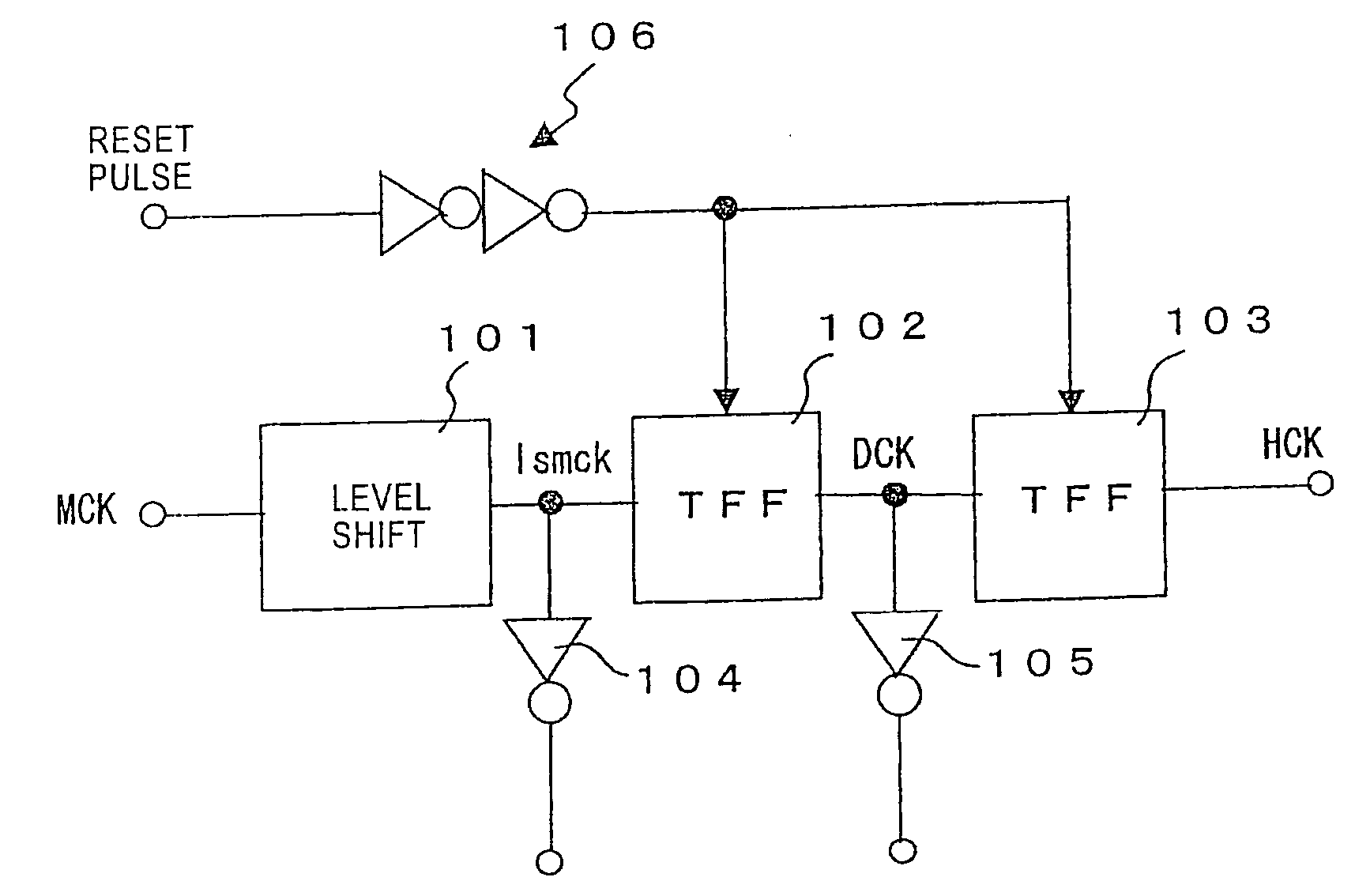
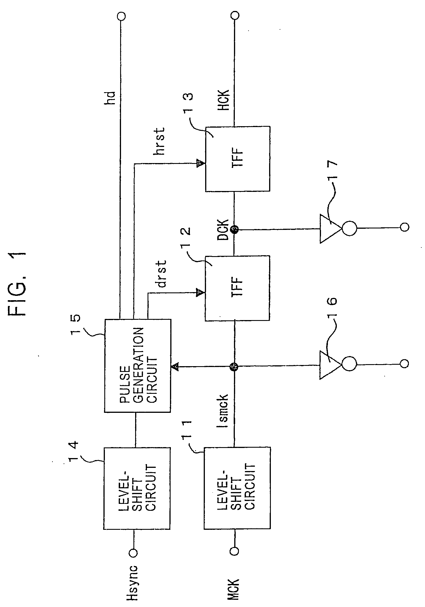
[0040]FIG. 4 is a block diagram showing an example of the configuration of a display device, for example, a liquid-crystal display device, according to the present invention. In FIG. 4, on a transparent insulating substrate, for example, a glass substrate 31, a display section (pixel section) 32 having pixels arranged thereon in a matrix is formed. The glass substrate 31 is opposedly arranged with a predetermined spacing with another glass substrate, and a display panel (LCD panel) is formed by sealing a liquid-crystal material between the two substrates.

[0041] An example of the structure of each pixel at the display section 32 is shown in FIG. 5. Each pixel 50 arranged in a matrix is configured to have a TFT (Thin-Film Transistor) 51, which is a pixel transistor; a liquid-crystal cell 52 whose pixel electrode is connected to the drain electrode of the TFT 51; and a holding capacitor 53, one of electrodes of which is connected to the drain electrode of the TFT 51. Here, the liquid-...


PUM


Abstract

When a buffer is formed by using transistors having large element characteristic variations, the deviation of the timing between the input clock pulse and the reset pulse is likely to occur. When the deviation of the timing becomes larger, a malfunction is caused to occur, and an operation margin becomes smaller with respect to the variations of the element characteristics. In a timing generation circuit, which is formed on an insulating substrate and which has two TFFs (12, 13), for generating a dot clock DCK and a horizontal clock HCK whose frequencies are different in synchronization with a master clock MCK which is input external to the substrate, separate reset pulses drst and hrst are generated at a pulse generation circuit 15 with respect to the two TFFs (12, 13), and a resetting operation is performed at separate timings. Thus, a large operation margin can be ensured even when each circuit is formed by using TFTs having large element characteristic variations and a rough process rule.

Description

TECHNICAL FIELD [0001] The present invention relates to a logic circuit, a timing generation circuit, a display device, and a portable terminal. More particularly, the present invention relates to a logic circuit which is formed on an insulating substrate by using transistors having large characteristic variations, a timing generation circuit using the logic circuit, a display device using the timing generation circuit as one of peripheral driving circuits, and a portable terminal having incorporated therein the display device as a screen display section. BACKGROUND ART [0002] A conventional example of a timing generation circuit, which is one type of logic circuit, is shown in FIG. 7. The timing generation circuit according to this conventional example is configured to have a level-shift circuit 101, and two flip-flops which are cascade-connected in sequence to the output thereof, that is, T-type flip-flops (hereinafter referred to as “TFFs”) 102 and 103 in this example. The level-...

Claims


Application Information

Patent Timeline
Patent Type & Authority Applications(United States)
IPC IPC(8): H03K19/00G09G3/20G09G3/36G09G5/18H01L29/786
CPCG09G2310/08G09G3/20G09G2310/0289G09G5/18G09G2300/0408G09G3/3648
Inventor KIDA, YOSHITOSHINAKAJIMA, YOSHIHARUMAEKAWA, TOSHIKAZU
Owner JAPAN DISPLAY WEST
Why Eureka
Try Eureka