Variable resistive element and nonvolatile semiconductor memory device

a resistive element and non-volatile technology, applied in the direction of semiconductor devices, bulk negative resistance effect devices, electrical equipment, etc., can solve the problems of not always employing material which can be easily used in the manufacturing process, difficult to perform the miniaturization process to provide high-integrated memory with this kind of material, etc., to reduce the variation in parasitic resistance due to process variation of the electrode, and reduce the variation in resistance change characteristics (switching characteristics

Inactive Publication Date: 2013-09-26
SHARP KK +1
View PDF1 Cites 3 Cited by
  • Summary
  • Abstract
  • Description
  • Claims
  • Application Information

AI Technical Summary

Benefits of technology

[0049]The inventors of the present invention have focused on a current flow from a contact point between the filament and the electrode to the electrode, or from the electrode to the contact point in the filament type variable resistive element, and found a guideline for reducing the variation in parasitic resistance caused by the variation in electrode dimension in the fine element, as a result of their earnest study.
[0050]Thus, as for the nonvolatile semiconductor memory device provided with fine variable resistive elements, the variation in parasitic resistance due to process variation of the electrode can be reduced, and it becomes possible to provide a highly integrated memory in which variation in resistance change characteristics (switching characteristics) is reduced and an operation margin is large.

Problems solved by technology

However, it is not clear how the parasitic resistance is controlled in the miniaturized filament type variable resistive element, and there is no guideline for a method for reducing the parasitic resistance at the present.
Thus, the material which can be easily used in the manufacturing process is not always employed as the electrode material.
The variable resistive element having the metal oxide as the variable resistor uses the electrode formed of noble metal such as Pt, Ru, or Ir in many cases, but the problem is that it is hard to perform the miniaturizing process to provide the highly integrated memory with this kind of material, or the material itself is expensive.
However, due to the constraint condition, the material having relatively high resistivity has to be employed as the electrode material in some cases.
When the material having high resistivity is used as the electrode material, the above-described parasitic resistance and the variation in parasitic resistance caused in the variable resistive element are increased as a matter of course, which causes the problem in providing the highly integrated memory.
Especially, when the resistivity of the electrode material is 100 μΩcm or more, the problem of the parasitic resistance value and the variation in parasitic resistance becomes serious, so that it is difficult to provide the highly integrated memory.

Method used


Image

  • Variable resistive element and nonvolatile semiconductor memory device
  • Variable resistive element and nonvolatile semiconductor memory device
  • Variable resistive element and nonvolatile semiconductor memory device

Examples


first embodiment

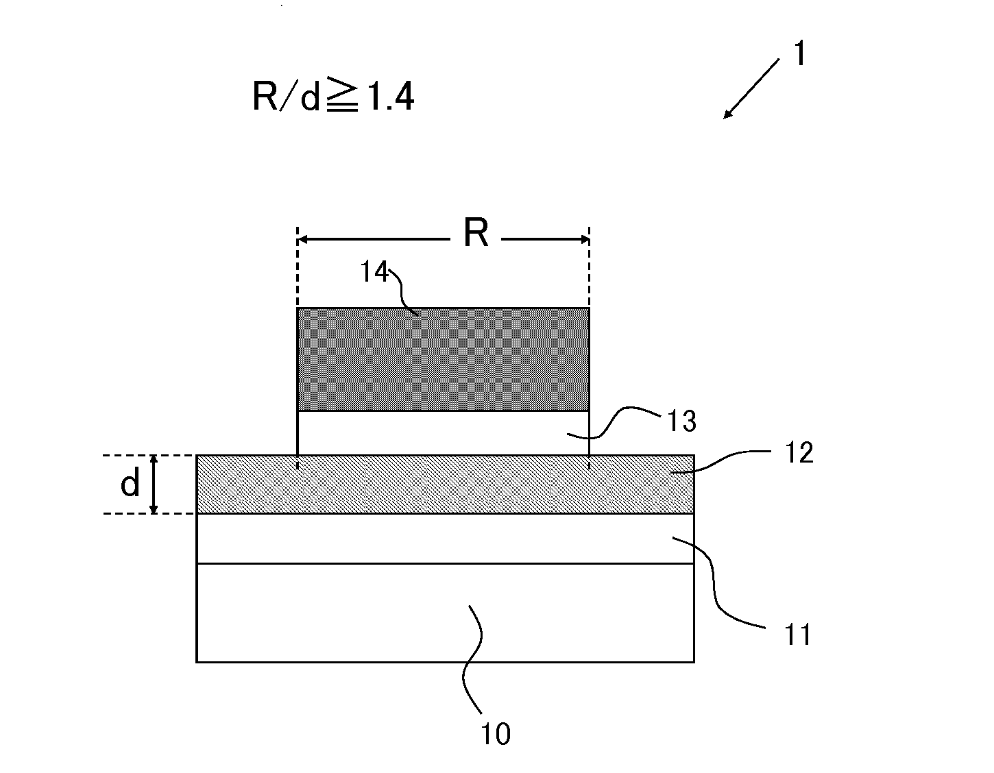
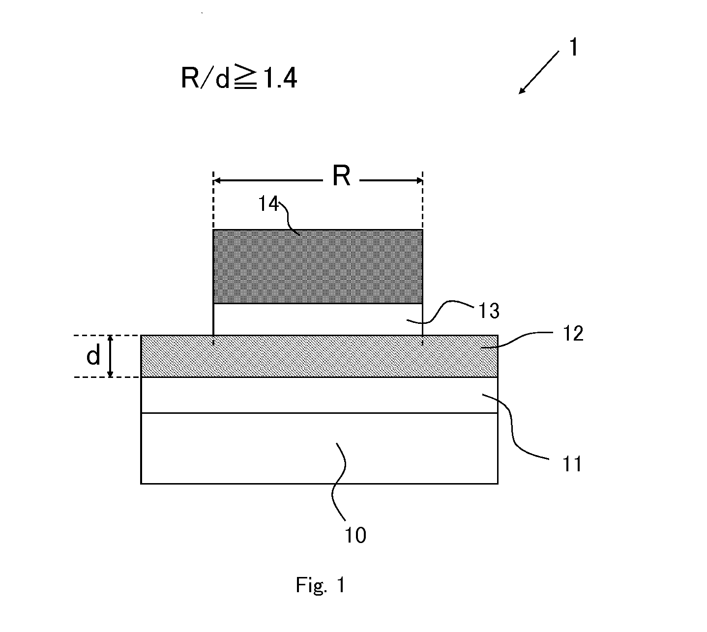
[0066]FIG. 1 is a sectional view schematically illustrating a structure of a variable resistive element 1 (hereinafter appropriately referred to as a “present element 1”) according to one embodiment of the present invention. In the drawings described below, essential parts are emphasized for the sake of convenience of description, and a dimensional ratio of each component of the element and an actual dimensional ratio do not agree with each other in some cases.

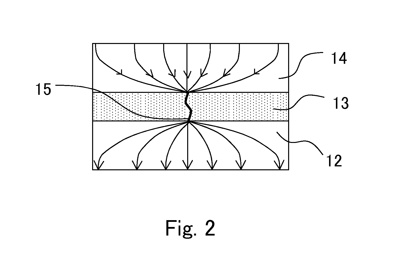
[0067]The variable resistive element 1 includes a second electrode (lower electrode) 12, a variable resistor 13, and a first electrode (upper electrode) 14, those of which are deposited and patterned in this order on an insulating film 11 formed on a substrate 10. The variable resistor 13 includes a layer which is made of a metal oxide or a metal oxynitride.

[0068]In the present embodiment, hafnium oxide (HfOX) that has a large bandgap and that is an insulating layer is selected to be used for the metal oxide serving as a varia...

second embodiment

[0098]FIG. 11 illustrates a non-volatile semiconductor memory device using the present elements 1 to 3 described above. FIG. 11 is a circuit block diagram illustrating a schematic configuration of a non-volatile semiconductor memory device 20 (hereinafter referred to as a “present device 20” as needed) according to one embodiment of the present invention. As illustrated in FIG. 11, the present device 20 includes a memory cell array 21, a control circuit 22, a voltage generating circuit 23, a word line decoder 24, a bit line decoder 25, a source line decoder 26, and a read circuit 27.

[0099]The memory cell array 21 includes a plurality of memory cells, each of which includes any one of the present elements 1 to 3 as a memory element, arranged in at least one of a row direction and a column direction in a matrix. The memory cells belonging to the same column are connected by a bit line extending in the column direction, and the memory cells belonging to the same row are connected by a ...


PUM


Abstract

As for a variable resistive element including first and second electrodes, and a variable resistor containing a metal oxide between the first and second electrodes, in a case where a current path having a locally high current density of a current flowing between the both electrodes is formed in the metal oxide, and resistivity of at least one specific electrode having higher resistivity of the both electrodes is 100 μΩcm or more, a dimension of a contact region of the specific electrode with the variable resistor in a short side or short axis direction is set to be more than 1.4 times as long as a film thickness of the specific electrode, which reduces variation in parasitic resistance generated in an electrode part due to process variation of the electrode, and prevents variation in resistance change characteristics of the variable resistive element generated due to the variation in parasitic resistance.

Description

CROSS REFERENCE TO RELATED APPLICATION[0001]This Nonprovisional application claims priority under 35 U.S.C. §119(a) on Patent Application No. 2012-065820 filed in Japan on Mar. 22, 2012 the entire contents of which are hereby incorporated by reference.BACKGROUND OF THE INVENTION[0002]1. Field of the Invention[0003]The present invention relates to a nonvolatile variable resistive element including a first electrode, a second electrode, and a layer serving as a variable resistor formed of a metal oxide and sandwiched between the above electrodes, and a nonvolatile semiconductor memory device using the variable resistive element for storing information.[0004]2. Description of the Related Art[0005]Recently, as a high-speed operable next-generation nonvolatile random access memory (NVRAM) to replace a flash memory, various device structures such as FeRAM (Ferroelectric RAM), MRAM (Magnetic RAM), and PRAM (Phase Change RAM) have been proposed, and they face intense development competition...

Claims


Application Information

Patent Timeline
Patent Type & Authority Applications(United States)
IPC IPC(8): H01L45/00
CPCH01L45/126H01L45/08H01L45/1233H01L27/2472H01L45/145H01L45/146H01L27/2436H01L45/1253H10B63/82H10B63/30H10N70/24H10N70/841H10N70/826H10N70/883H10N70/8833H10N70/8413
Inventor TAMAI, YUKIONAKANO, TAKASHIAWAYA, NOBUYOSHIAIZAWA, KAZUOASANO, ISAMUHIGANO, NAOYAKAWAGOE, TSUYOSHI
Owner SHARP KK
Why Eureka
Try Eureka