Semiconductor memory device and test method therefor
a memory device and semiconductor technology, applied in the direction of information storage, static storage, digital storage, etc., can solve the problems of increasing the deviation of the snm, excessive operation margin, and more difficult to secure the operation margin, and achieve excellent productivity
- Summary
- Abstract
- Description
- Claims
- Application Information
AI Technical Summary
Benefits of technology
Problems solved by technology
Method used
Image


Examples
first exemplary embodiment
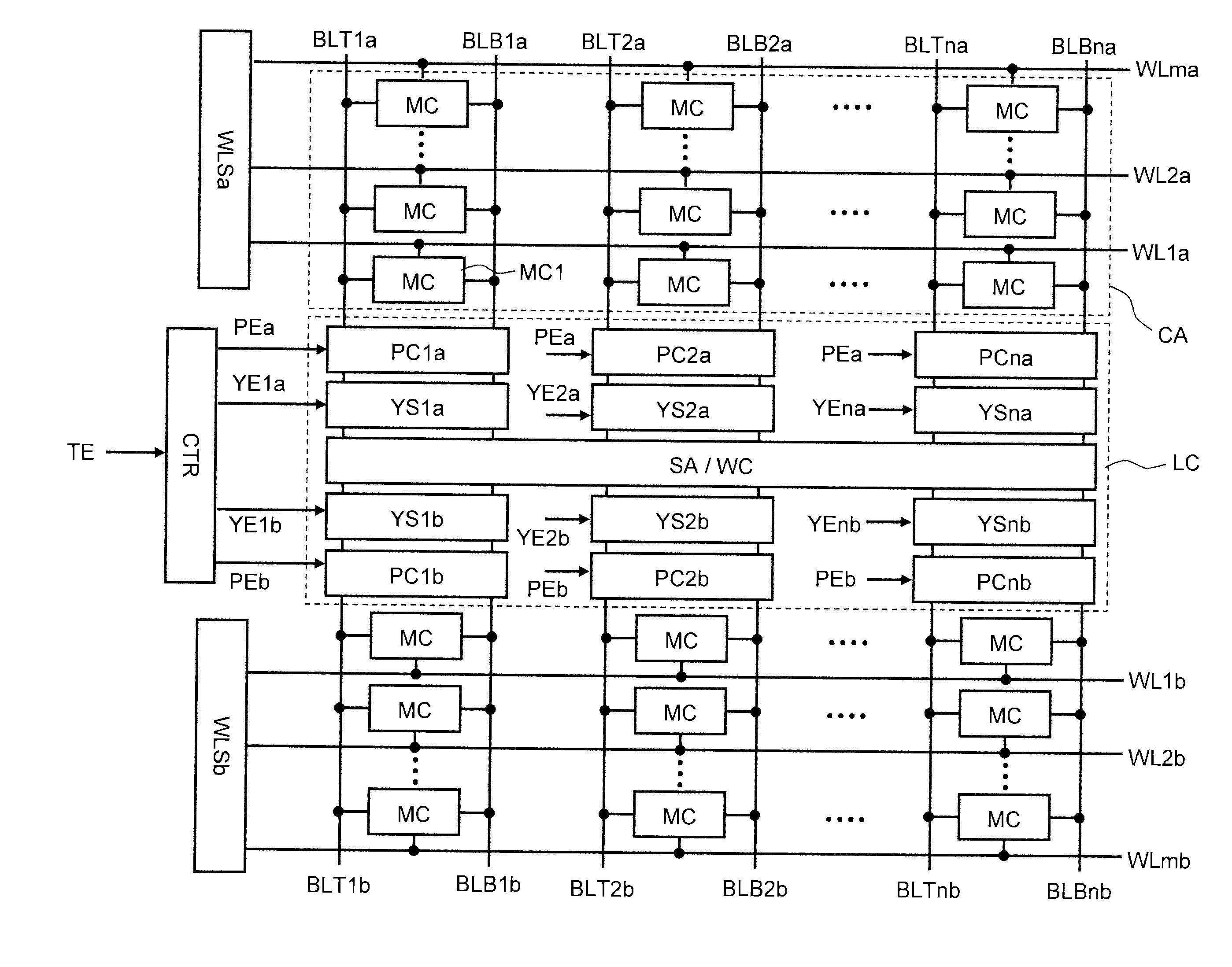
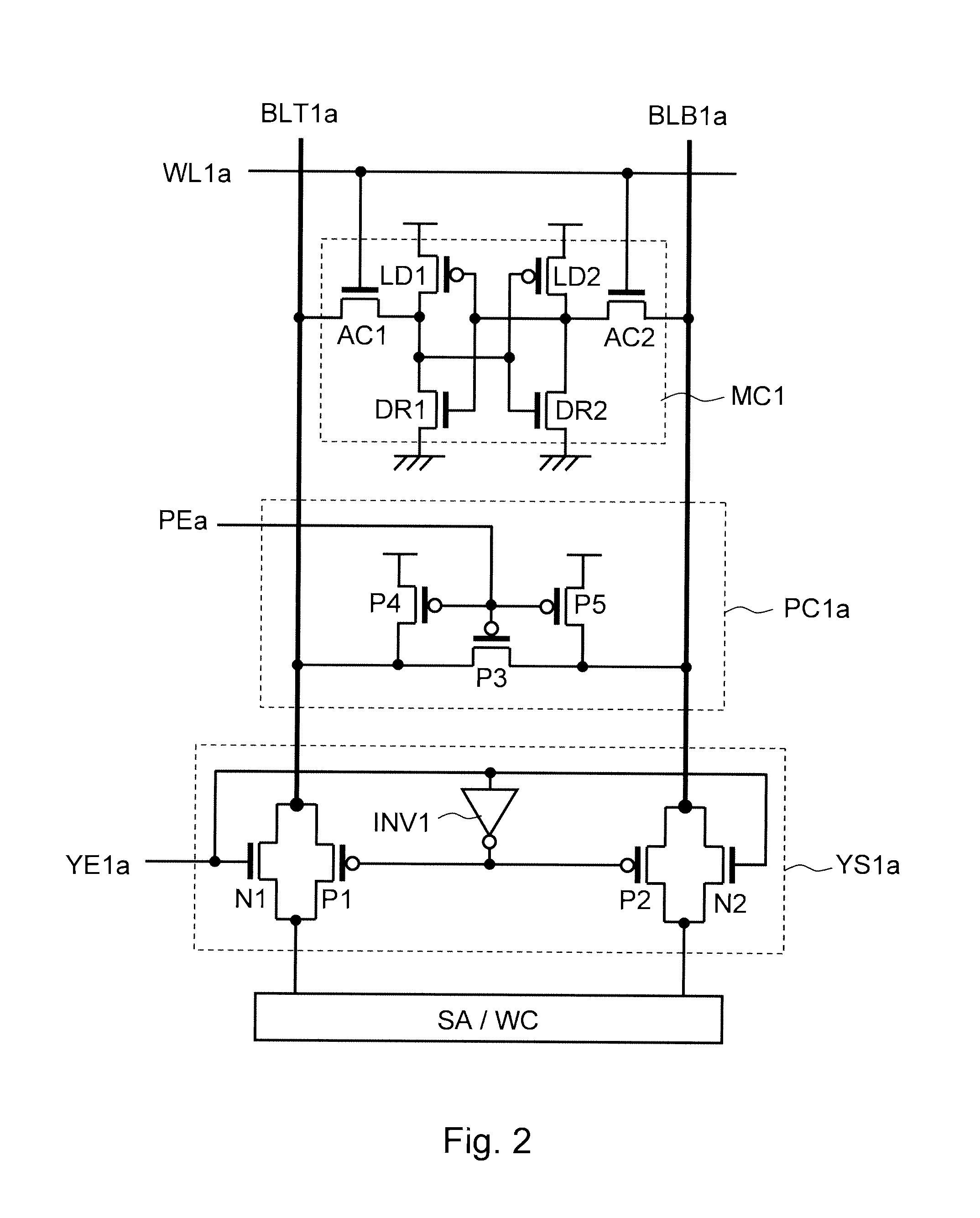
[0031]FIG. 1 is a circuit diagram illustrating a semiconductor memory device according to a first exemplary embodiment of the present invention. The semiconductor memory device is an SRAM. The semiconductor memory device includes a control circuit CTR, a sense amplifier SA, a write circuit WC, n (n is a natural number) pairs of Y selectors YSla to YSna and YS1b to YSnh, n pairs of precharge circuits PC1a to PCna and PC1b to PCnb, 2n pairs of bit lines BLT1a and BLB1a to BLTna and BLBna, and BLT1b and BLB1b to BLTnb and BLBnb, a pair of word line selectors WLSa and WLSb, m (m is a natural number) pairs of word lines WL1a to WLma and WL1b to WLmb, and n×m pairs of memory cells MC. The sense amplifier and write circuit SA / WC includes the sense amplifier SA and the write circuit WC which are integrally illustrated in FIG. 1 for convenience of illustration. The sense amplifier SA is a circuit that amplifies a potential difference between two sense nodes of a memory cell MC selected in a ...
second exemplary embodiment
[0066]Next, a second exemplary embodiment of the present invention will be described with reference to FIG. 8. FIG. 8 is a circuit diagram illustrating a semiconductor memory device according to the second exemplary embodiment. The semiconductor memory device shown in FIG. 8 differs from the semiconductor memory device shown in FIG. 1 in that bridge circuits BLG for connecting the bit line pairs which are opposed to each other through the local circuit LC are provided for each bit line pair. The other configurations are similar to those of the first exemplary embodiment, so the description thereof is omitted.
[0067]Specifically, the bit line pair BLT1a and BLB1a and the bit line pair BLT1b and BLB1b are connected through the bridge circuit BLG without involving the sense amplifier SA. That is, between the bit line pair BLT1a and BLB1a and the bit line pair BLT1b and BLB1b, the bridge circuit BLG and the sense amplifier SA are connected in parallel with each other. Similarly, a bit li...
third exemplary embodiment
[0071]Next, a third exemplary embodiment of the present invention will be described with reference to FIG. 10. FIG. 10 is a circuit diagram illustrating a semiconductor memory device according to the third exemplary embodiment. The semiconductor memory device shown in FIG. 10 includes two circuits shown in FIG. 1, and the two circuits are connected through the bridge circuits BLG.
[0072]On both sides of the local circuit LC1, cell arrays CAa and CAb are connected to each other. Similarly, on both sides of the local circuit LC2, cell arrays CAc and CAd are connected to each other. Additionally, word line selectors WLSb, WLSc, and WLSd are connected to the cell arrays CAb, CAc, and CAd through word lines WLb, WLc, WLd, respectively. Note that the word lines WLb, WLc, and WLd are each represented by one line for convenience of illustration. The detailed configurations of the local circuits LC1 and LC2 and the cell arrays CAa, CAb, CAc, and CAd are similar to those of FIG. 1.
[0073]The ce...
PUM
 Abstract
Description
Claims
Application Information
 - R&D
- Intellectual Property
- Life Sciences
- Materials
- Tech Scout
- Unparalleled Data Quality
- Higher Quality Content
- 60% Fewer Hallucinations
Browse by: Latest US Patents, China's latest patents, Technical Efficacy Thesaurus, Application Domain, Technology Topic, Popular Technical Reports.
© 2025 PatSnap. All rights reserved.Legal|Privacy policy|Modern Slavery Act Transparency Statement|Sitemap|About US| Contact US: help@patsnap.com