Method for manufacturing absorber layers for solar cell
- Summary
- Abstract
- Description
- Claims
- Application Information
AI Technical Summary
Benefits of technology
Problems solved by technology
Method used
Image

Examples
first embodiment
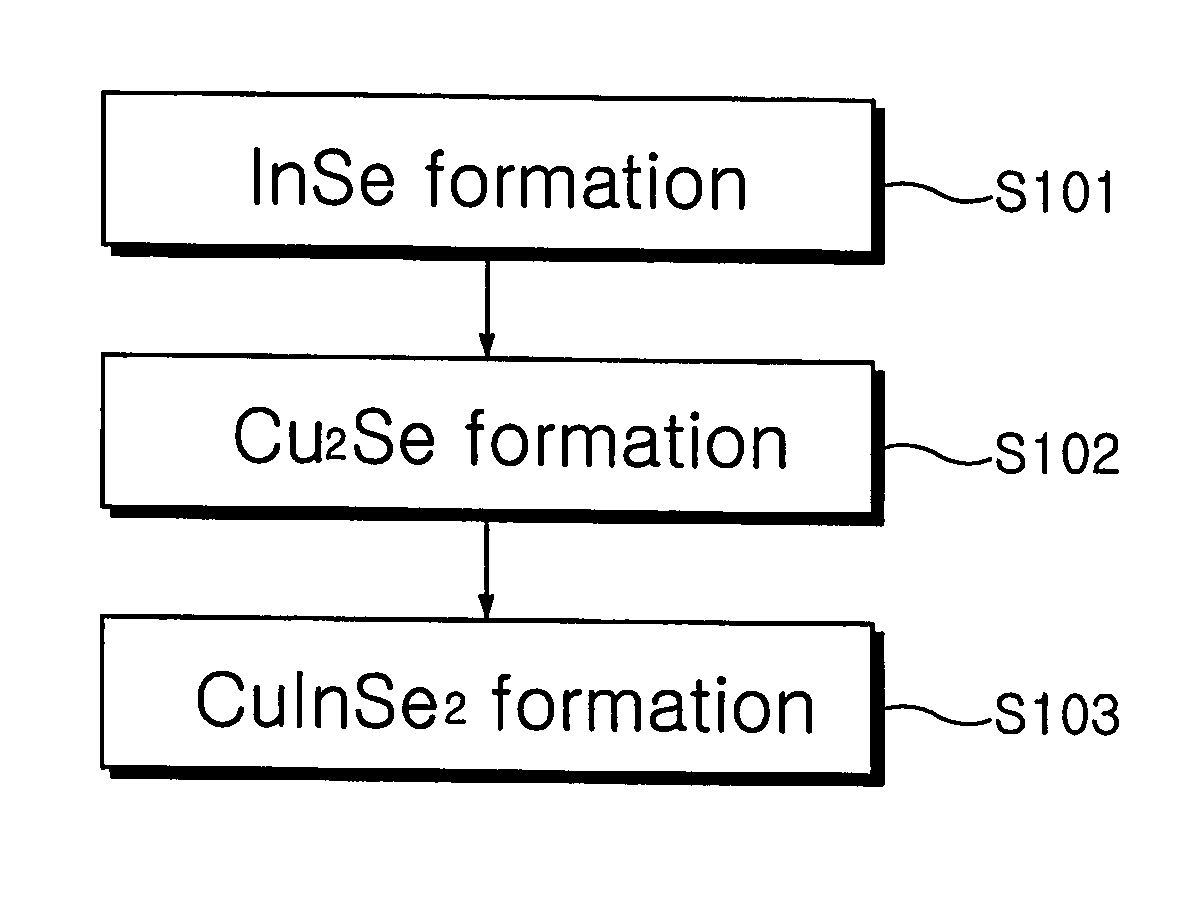
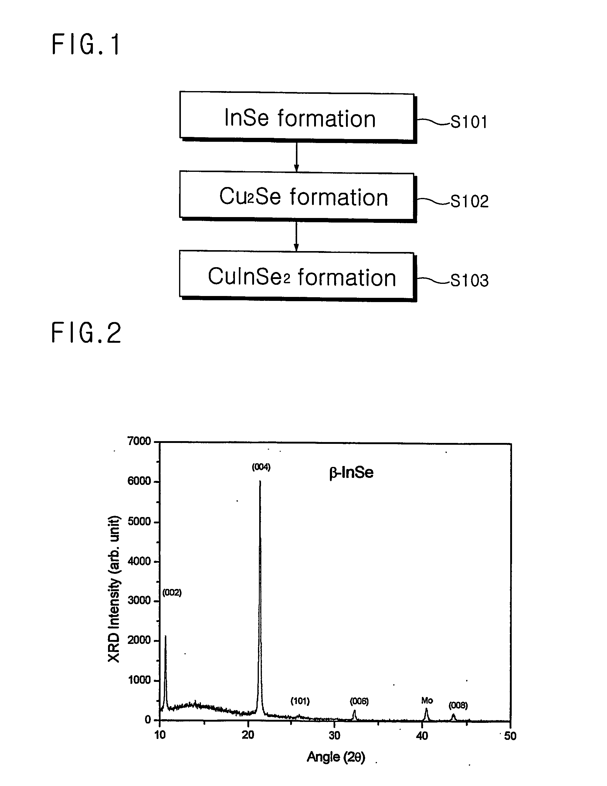
[0024]FIG. 1 schematically illustrates a process flow for production of a CIS thin film in accordance with the present invention;
[0025] As shown in FIG. 1, an InSe thin film is formed on a substrate made of Mo material by MOCVD using [Me2In-(μSeMe)]2, a single precursor including In and Se (step S101). Me represents methyl, and U means that Se is double-bonded to In. As the substrate, a thin and flexible substrate made of the Mo material may be used instead of a conventional glass substrate, and thus various shapes of solar cells may be implemented.
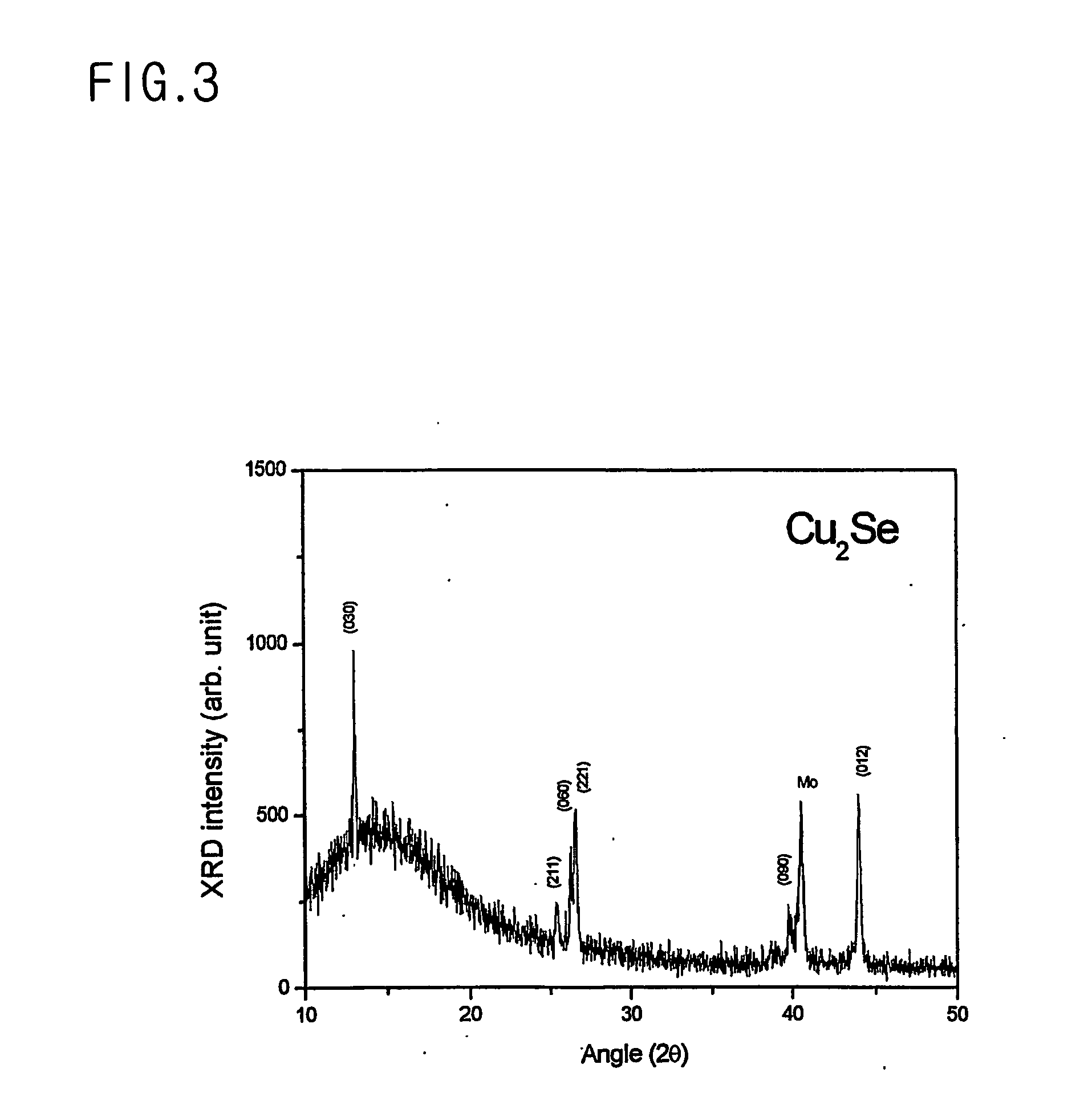
[0026] Next, a Cu2Se thin film is formed on the InSe thin film formed in step S101 by MOCVD using a monovalent Cu precursor (hfac)Cu(DMB) (step S102). The hfac and DMB are abbreviations of hexafluoroacetylacetonate and 3,3-dimethyl-1-butene, respectively.
[0027] Next, a CuInSe2 thin film is formed on the Cu2Se thin film formed in step S102 by MOCVD using [Me2In-(μSeMe)]2, a single precursor including In and Se (step S103). [Me2In-(μSeMe)...
second embodiment
[0032]FIG. 5 shows a process flow schematically illustrating production of a CIGS thin film in accordance with the present invention.
[0033] As shown in FIG. 5, steps S201 through S203 are the same as in the above-mentioned CIS thin film production process. A CuIn1-xGaxSe2 thin film is formed on the CuInSe2 thin film formed in step S203 by MOCVD using [Me2Ga-(μSeMe)]2, a precursor including Ga and Se (step S204). [Me2Ga-(μSeMe)]2 is a precursor material wherein In in [Me2In-(μSeMe)]2 was replaced with Ga.
[0034] In order to analyze physical properties with regard to In and Ga composition ratio of the grown CIGS thin film, 5 samples (A, B, C, D and E) having different composition ratios were prepared by differing a vapor deposition period of time in step S204 so as to adjust the composition ratio of In and Ga. In the CuIn1-xGaxSe2 thin film, a value of x, i.e., the composition ratio of [Ga] / [In+Ga] was examined by X-ray fluorescence spectroscopy thus showing 0, 0.062, 0.19, 0.34 and 0...
PUM
 Abstract
Description
Claims
Application Information
 - R&D
- Intellectual Property
- Life Sciences
- Materials
- Tech Scout
- Unparalleled Data Quality
- Higher Quality Content
- 60% Fewer Hallucinations
Browse by: Latest US Patents, China's latest patents, Technical Efficacy Thesaurus, Application Domain, Technology Topic, Popular Technical Reports.
© 2025 PatSnap. All rights reserved.Legal|Privacy policy|Modern Slavery Act Transparency Statement|Sitemap|About US| Contact US: help@patsnap.com