Transistor

Inactive Publication Date: 2006-09-14
FUJI ELECTRIC HLDG CO LTD
View PDF12 Cites 39 Cited by
  • Summary
  • Abstract
  • Description
  • Claims
  • Application Information

AI Technical Summary

Benefits of technology

[0027] Various metal oxides such as the oxides of silicon, aluminum, tantalum, titanium, strontium and barium, anodic oxide films of these metals, and mixed oxides of these metals are used for the gate insulator film. Polymers such as polystyrene, poly(vinyl alcohol), poly(vinyl phenol) and an acrylic polymer may be used for the gate insulator film. Since the dielectric permeability of many metal oxides is higher than the dielectric permeability of the polymer materials, the metal oxide gate insulator film facilitates driving the transistor with a relatively low voltage. In contrast, since the dielectric permeability of the polymer material is relatively low, the polymer gate insulator film facilitates high-speed response.
[0035] As described in detail below, the organic thin film transistor according to the invention facilitates accumulating electric charges in the channel on the gate insulator film and realizing a high response frequency.

Problems solved by technology

Due to this light emission efficiency lowering, the electric power consumption in the passive matrix type driving system is larger than the electric power consumption in the active matrix type driving system, if the two are compared with each other at the same display luminance.
If the current that flows to the organic EL device is increased, the materials in the organic EL device will be deteriorated by heat generation and the life of the organic EL device will be shortened.
To obtain the same display luminance, it is necessary to increase the light emitting period, if the maximum current made to flow to the organic EL device is limited to obtain high light emission efficiency and a long device life.
However, since the duty ratio that determines the light emitting period for the passive matrix type driving system is inversely proportional to the number of pixel lines on the panel, an increased light emitting period limits the display capacity (the number of drivable lines).
However, the process temperature for forming a TFT that uses polysilicon is 250° C. or higher, which makes it hard to use a flexible plastic substrate.
However, various problems are posed by the organic thin film transistor.
The modulation frequency at which the current between the source and the drain is modulated with the gate voltage in the organic thin film transistor is still low, and the low modulation frequency is very hazardous when using an organic thin film transistor in practice.
Therefore, when the film thickness is thin it is impossible for the organic electronic material to cover the entire substrate surface, and this causes spatial defects 22.
Therefore, it is necessary for the organic electronic material film to be thicker than a certain value, and the above described problem has not been solved yet.
However, it is hard to control the concentration of the oxygen used for an electron acceptor.
Moreover, since it is impossible to suppress the current in the OFF-state, the ON / OFF ratio is low.
However, when the metallic material for the carrier generating layer is deposited on the film of an organic material by vacuum deposition or a similar deposition method, the organic material will be damaged by the heat caused by the vacuum deposition, thereby deteriorating the organic electronic material and impairing its properties.
In other words, the time constant determined by the electrostatic capacitance of the gate insulator film and the electrical resistance of the path, through which electric charges are accumulated in the electrostatic capacitance, are the factors which limit the frequency characteristics of the transistor, and pose a serious problem.

Method used


Image

  • Transistor
  • Transistor
  • Transistor

Examples


embodiment 1

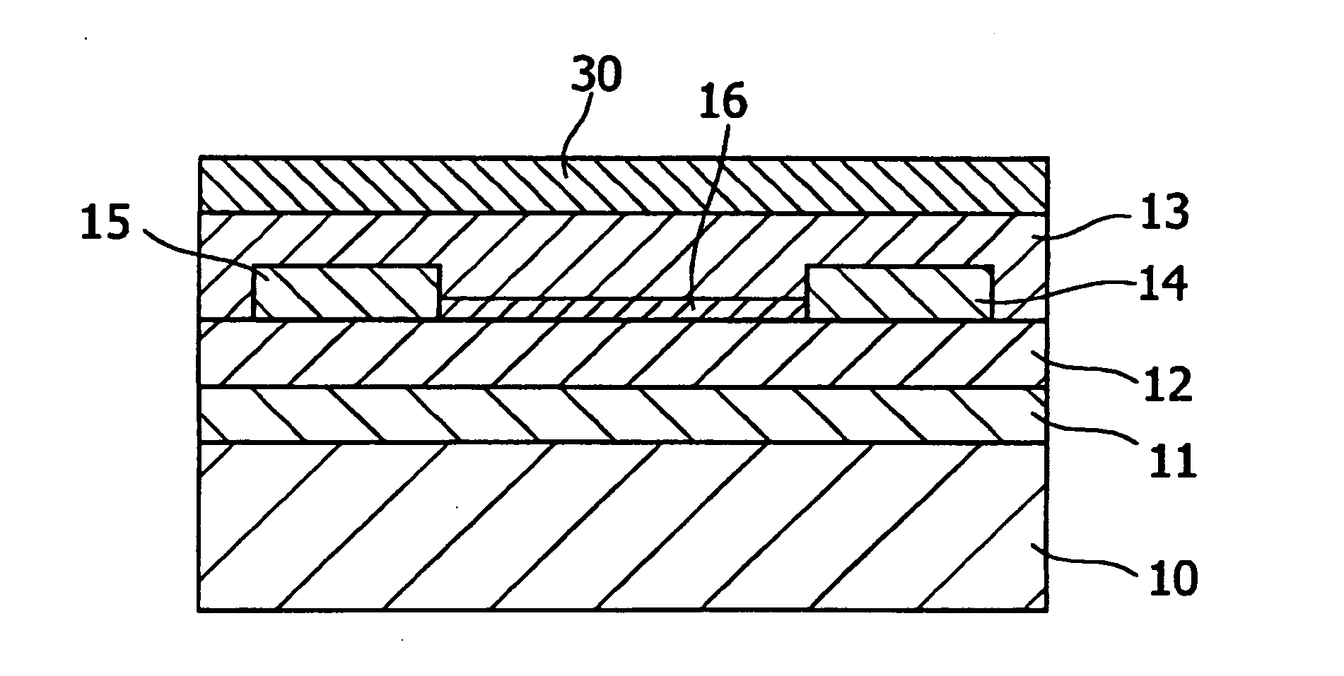
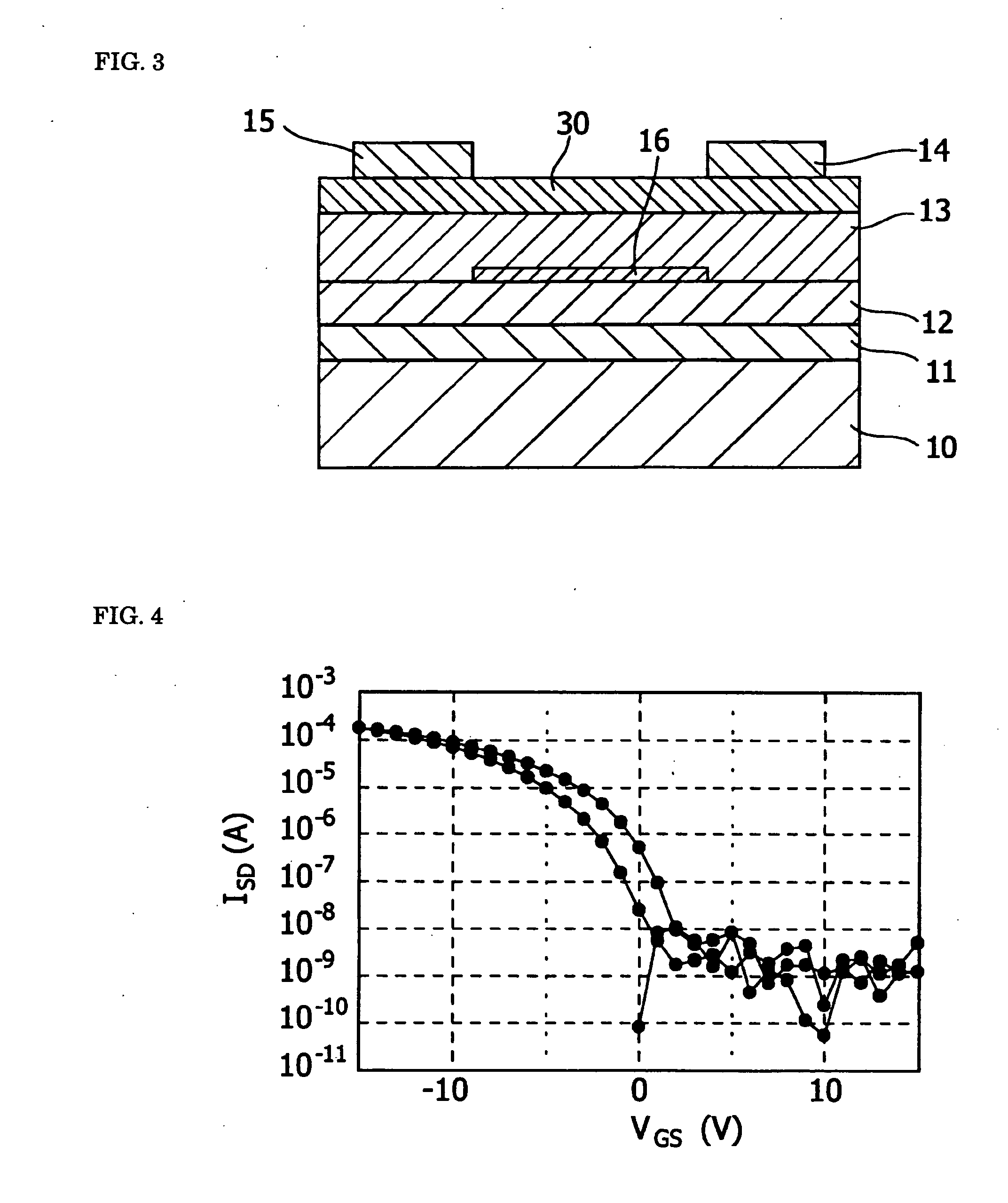
[0058] Tantalum gate electrode 11 is formed on glass substrate 10 by the usual photo-process and sputtering, resulting in gate electrode 11 of 150 nm in thickness. Then, an anodic oxide film is formed on gate electrode 11. The anodic oxidation is conducted in a solution containing 1 wt % of ammonium borate under the voltage of 70 V for 50 min, resulting in a gate insulator film 12 of 80 nm in thickness.

[0059] Then, source electrode 15 and drain electrode 14 are formed of gold vacuum deposition films. The gold film thickness is 80 nm. The channel is 5 μm in length and 100 μm in width. Next, first organic electronic material film 13 of 60 nm in thickness is formed by depositing an acenic compound having the structure described by the structural formula (1-18) (pentacene: supplied from Sigma-Aldrich Corporation) by the vacuum deposition method. The substrate temperature for depositing first organic electronic material film 13 is set at 60° C. Then, second organic electronic material f...

embodiment 2

[0061] An organic thin film transistor according to an embodiment 2 is fabricated in the same manner as the organic thin film transistor according to the embodiment 1 except that second organic electronic material film 30 in the organic thin film transistor according to the embodiment 2 contains 95 atomic % of pentacene (supplied from Sigma-Aldrich Corporation) and 5 atomic % of F4TCNQ (supplied from Sigma-Aldrich Corporation).

embodiment 3

[0062] An organic thin film transistor according to an embodiment 3 is fabricated in the same manner as the organic thin film transistor according to the embodiment 1 except that second organic electronic material film 30 in the organic thin film transistor according to the embodiment 3 contains 90 atomic % of pentacene (supplied from Sigma-Aldrich Corporation) and 10 atomic % of F4TCNQ (supplied from Sigma-Aldrich Corporation).


PUM


Abstract

A thin film field effect transistor is disclosed that includes a gate electrode, a gate insulator film the on gate electrode, and a first organic electronic material film containing a first organic electronic material on the gate insulator film. A source electrode and a drain electrode are spaced apart from each other on the first organic electronic material film. The first organic electronic material film includes a portion between the source electrode and the drain electrode that is in contact with the gate insulator film. This portion provides a current path. The current is controlled by the potential of the gate electrode. There is a second organic electronic material film that is in contact with the surface of first organic electronic material film opposite to the portion that provides the current path. The second organic electronic material film contains a second organic electronic material and an electron acceptor or an electron donor. The thin film field effect transistor facilitates accumulating electric charges in the channel on the gate insulator film and realizing a high response frequency.

Description

CROSS REFERENCE TO RELATED APPLICATIONS [0001] This application claims priority from application Ser. Nos. JP 2005-012458, filed on Jan. 20, 2005 and JP2005-044010, filed on Feb. 21, 2005, the contents of which are incorporated herein in their entirety. BACKGROUND OF THE INVENTION [0002] A. Field of the Invention [0003] The present invention relates to thin film transistors which use organic electronic materials. [0004] B. Description of the Related Art [0005] Recently, flat panel displays for information equipment are spreading remarkably. Among the flat panel displays, the liquid crystal display controls the ON and OFF of the back lights utilizing the optical shutter function of the liquid crystal, and obtains colors using color filters. In contrast to this, every pixel in the organic EL display (or the organic LED display) emits light. Therefore, the view angle for the organic EL display is wide. Moreover, since the organic EL display does not need any back light, it is possible ...

Claims


Application Information

Patent Timeline
IPC IPC(8): H01L29/08
CPCH01L21/31683H01L51/001H01L51/0051H01L51/0052H01L51/0545H01L51/0562H01L51/0583H10K71/164H10K85/611H10K85/615H10K10/486H10K10/466H10K10/26H01L21/02244
Inventor KAWAKAMI, HARUOKATO, HISATOMAEDA, TAKAHIKOSEKINE, NOBUYUKI
Owner FUJI ELECTRIC HLDG CO LTD
Why Eureka
Try Eureka