Anode for nonaqueous secondary battery, process of producing the anode, and nonaqueous secondary battery
a secondary battery and anode technology, applied in the manufacturing process of electrodes, cell components, coatings, etc., can solve the problems of battery using the negative electrode having a reduced cycle life, battery using the negative electrode tending to have a remarkable increase in power consumption, and the active material in the negative electrode is relatively small
- Summary
- Abstract
- Description
- Claims
- Application Information
AI Technical Summary
Benefits of technology
Problems solved by technology
Method used
Image
Examples
example 1-1
(1) Preparation of Active Material Particles
[0123] A molten metal at 1400° C. containing 80% of silicon and 20% of nickel was cast into a copper-made mold and quenched to obtain an ingot of a silicon-nickel alloy. The ingot was ground in a jet mill and sieved to obtain active material particles. The particles had an average particle size (D50) of 5 μm.
(2) Preparation of Slurry
[0124] A slurry having the following composition was prepared.
Active material particles obtained in (1) above16%Acetylene black (particle size: 0.1 μm)2%Binder (polyvinylidene fluoride)2%Diluting solvent (N-methylpyrrolidone)80%
(3) Formation of Release Layer
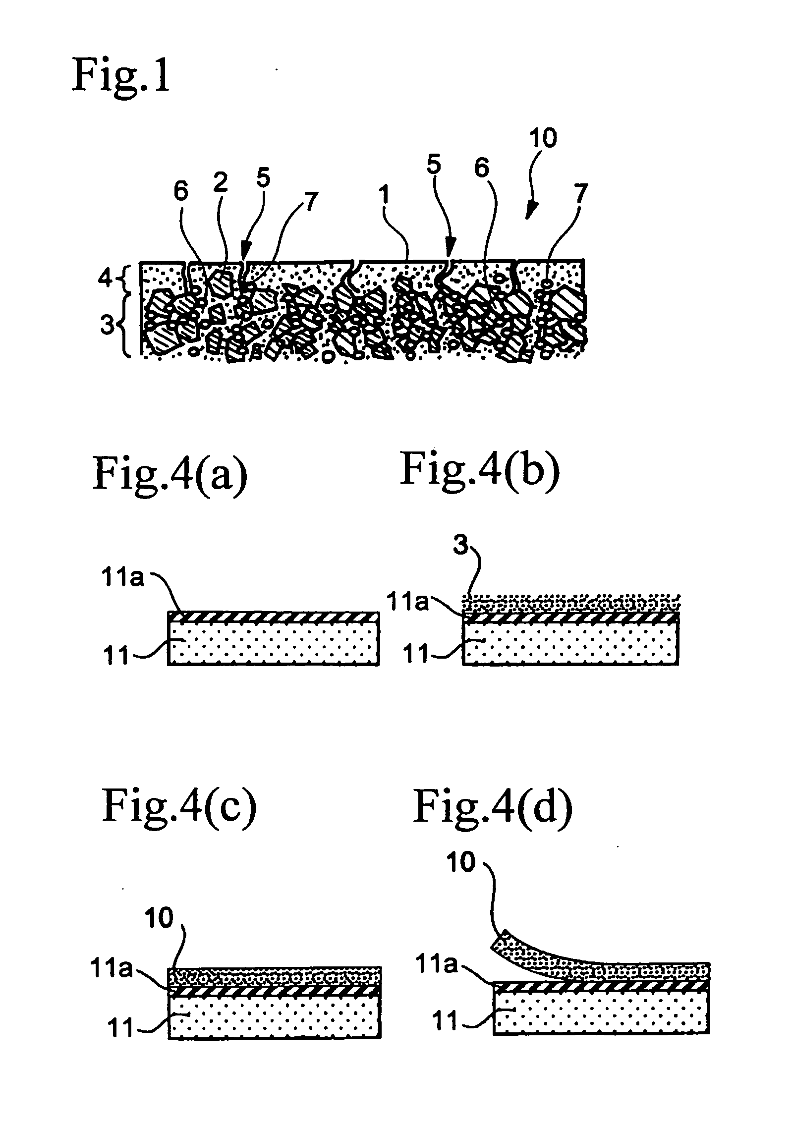
[0125] A surface of an electrolytically prepared copper carrier foil (thickness: 35 μm; surface roughness Ra: 0.1 μm) was treated with a chromate to form a 0.5 μm thick release layer (see FIG. 4(a)). The release layer also had a surface roughness Ra of 0.1 μm.
(4) Formation of Active Material Layer
[0126] The above prepared slurry was applied to th...
example 1-2
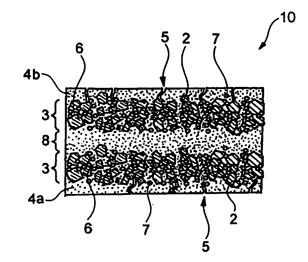
[0130] A negative electrode was obtained in the same manner as in Example 1-1, except for changing the electroplating time to 60 seconds. The first surface layer and the second surface layer had a thickness of 1 μm and 0.5 μm, respectively. Each of the surface layers was found to have a great number of microvoids which opened on the surface of the surface layer and led to the active material layer. The average opening area and the open area ratio of the microvoids were as shown in Table 1-1.
example 1-3
[0131] A negative electrode was obtained in the same manner as in Example 1-1, except for changing the electroplating time to 130 seconds. The first surface layer and the second surface layer had a thickness of 1 μm and 5 μm, respectively. Each of the surface layers was found to have a great number of microvoids which opened on the surface of the surface layer and led to the active material layer. The average opening area and the open area ratio of the microvoids were as shown in Table 1-1.
PUM
| Property | Measurement | Unit |
|---|---|---|
| thickness | aaaaa | aaaaa |
| open area ratio | aaaaa | aaaaa |
| particle diameter | aaaaa | aaaaa |
Abstract
Description
Claims
Application Information
 - R&D
- Intellectual Property
- Life Sciences
- Materials
- Tech Scout
- Unparalleled Data Quality
- Higher Quality Content
- 60% Fewer Hallucinations
Browse by: Latest US Patents, China's latest patents, Technical Efficacy Thesaurus, Application Domain, Technology Topic, Popular Technical Reports.
© 2025 PatSnap. All rights reserved.Legal|Privacy policy|Modern Slavery Act Transparency Statement|Sitemap|About US| Contact US: help@patsnap.com


