
Transfer optical surface machining method, optical device producing mold and optical device

a technology of optical surface and machining method, which is applied in the direction of turning machine accessories, drilling tools, manufacturing tools, etc., can solve the problems of increasing the number of pixels of the image capture device, further miniaturization of the device, and high initial performance of the optical device, so as to prolong the service life of the tool, reduce the number of tools, and reduce the effect of chipping

Active Publication Date: 2006-06-08
KONICA MINOLTA INC
View PDF8 Cites 30 Cited by
  • Summary
  • Abstract
  • Description
  • Claims
  • Application Information

AI Technical Summary

Benefits of technology

[0015] The object of the present invention is to solve the aforementioned problems and to provide a transfer optical surface machining method, wherein, when machining the material of high hardness used in an optical device producing mold, the chipping of a tool can be minimized to prolong the service life of the tool, and the transfer optical surfaces of multiple optical device producing molds can be cut to high precision, using one tool. The aforementioned object of the present invention also includes providing an optical device producing mold machined by the aforementioned method, and an optical device formed thereby.

Problems solved by technology

There has been an increase in the number of pixels of the image capturing device, and further miniaturization of the device.
In this context, it is not sufficient that the initial performance of the optical device is high.
At this temperature, the mirror surface cannot be maintained in the atmosphere due to oxidation, even in the case of a heat-resistant metallic material.
The high-hardness material of such a GM producing mold is very difficult to process in order to get the transfer optical surface.
Accordingly, a uniform structure cannot be obtained when viewed from a microscopic scale.
It is difficult to manufacture a wheel contour with high precision.
Accordingly, the machined contour is easily subjected to an error due to the wheel contour error.
Further, the binder does not have much hardness, and is subjected to elastic deformation due to the force applied to the wheel during the machining.
Thus, on a microscopic scale, grinding does not provide a method of transferring the precision of movement by forced infeed; it rather provides pressure transfer.
Machining precision can hardly be improved if the machine movement precision and tool rotary precision have been improved.
Thus, the contour precision of the produced wheel is not very satisfactory.
Not only that, the binder may be cracked by scraping.
Force may have been applied to the diamond abrasive grains to disengage them, and the diamond abrasive grains may be kept unstable.
The surrounding binder is damaged by excessive movement at the time of scraping the binder.
Such a phenomenon occurs to the surface of the wheel, which is kept very unstable.
The conventional concept of dressing such a tool of rough structure by the aforementioned rough method has been unfitted for high-precision, high-accuracy machining of the transfer optical surface.
Further, grinding is based on the self-regenerating function of the cutting blade resulting from wear of the wheel.
A contour error occurs on the transfer optical surface having been produced.
Machining of a high-precision transfer optical surface is difficult due to rapid wear of the wheel.
However, chipping of the diamond tool tends to occur, when cutting a material of high hardness using a diamond tool.
If the tool is chipped, a uniform and continuous surface cannot be obtained after cutting.
The required contour precision of the transfer optical surface cannot be maintained.
Such a problem of chipping may occur to other tools than a diamond tool.

Method used


Image

  • Transfer optical surface machining method, optical device producing mold and optical device
  • Transfer optical surface machining method, optical device producing mold and optical device
  • Transfer optical surface machining method, optical device producing mold and optical device

Examples


example 1

[0163] The inventors of the invention practiced the method of processing of the invention by using the superfine processing machine shown in FIG. 11. Tungsten carbide (hereinafter referred to as WC) of RCC-FN (Vickers hardness Hv=2500) manufactured by Nippon Tungsten Co., Ltd. was used as a material of the workpiece. A form of an aspheric surface transfer optical surface representing an object to be processed is a concave transfer optical surface that is small and deep having approximate R concave of about 0.9 mm, central radius of curvature of 1.4 mm and an angle of maximum likelihood of 65°.

[0164] A surface to become a transfer optical surface on the workpiece was processed by electrical discharge machining in advance to become a concave spherical surface, and was further machined roughly to become a form of aspheric surface from an approximate aspheric surface, by a general purpose precision grinding machine having an axial resolution of about 100 mm. In this roughing grinding p...

example 2

[0176] The inventors of the invention conducted cutting operations by using the superfine processing machine shown in FIG. 8. Microalloy F (Vickers hardness Hv=1850) manufactured by Tungaloy Corporation was used as a material of a workpiece. With respect to a processed form to become a transfer optical surface, its cross-sectional form is in a form of an aspheric surface, and in the direction perpendicular to the processed form, it is in a cylindrical aspheric surface having no curvature (cross-sectional form in the Z-axis direction: approximate R concave of 3.2 mm, central radius of curvature of 5.4 mm, width of 0.9 mm, form in the X-axis direction: radius of curvature ∞ (infinite) and length of 15 mm).

[0177] In the same way as in Example 1, a transfer optical surface was processed by electrical discharge machining, and was machined roughly by a general purpose precision grinding machine. Finishing cutting operations of the invention was conducted by the superfine processing machi...

example 3

[0186] The inventors of the invention conducted cutting operations of the invention by using the superfine processing machine of a biaxial type with X axis and Z axis shown in FIG. 9. As a material of a workpiece, SiC subjected to powder sintering was made to be a base material, and SiC was applied to a portion that is to be a transfer optical surface by CVD (which is called CVD-SiC film) to create an elaborate transfer optical surface. The hardness of CVD-SiC used this time was Vickers hardness Hv2800.

[0187] As a method of processing a transfer optical surface, grinding operations are conducted by a general purpose precision grinding machine at a form error of about 100 μmPV to a form of aspheric surface wherein a film thickness of CVD-SiC is considered. After that, CVD-SiC is coated to a thickness of about 500 μm. After coating, the transfer optical surface form is created by the general purpose precision grinding machine, while conducting correcting processing for the final asph...


PUM

PropertyMeasurementUnit
angleaaaaaaaaaa
angleaaaaaaaaaa
angleaaaaaaaaaa

Abstract

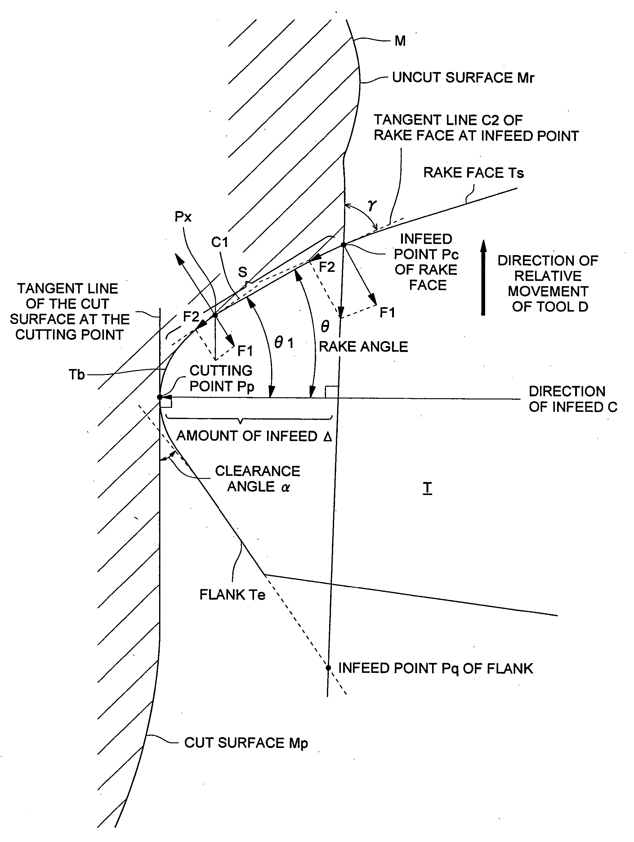
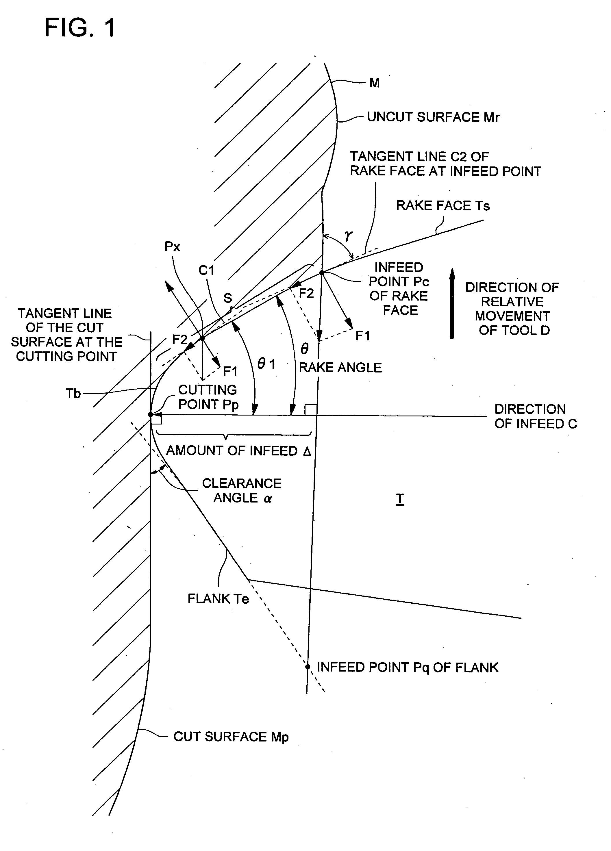
A machining method of machining a transfer optical surface on a optical element producing die having the transfer optical surface made of a material having Vickers hardness of Hv1500 or more, comprising: machining the transfer optical surface on the optical element producing die by cutting with a cutting tool, wherein a rake face of a tip of a blade of the cutting tool is set with an angle of minus values at an incising point on a surface to be machined.

Description

[0001] This application is based on Japanese Patent Application No. 2004-352368 filed on Dec. 6, 2004, in Japanese Patent Office, the entire content of which is hereby incorporated by reference. BACKGROUND OF THE INVENTION [0002] The present invention relates to a transfer optical surface machining method, an optical device producing mold and an optical device. More specifically, this invention relates to a method of machining the transfer optical surface of an optical device producing mold characterized by a high degree of hardness, suitable for a glass mold, to the optical device producing mold manufactured by using the same, and to the optical device produced using the same. [0003] In the prior art, the most popular method of producing an optical device is injection molding of plastic materials. Injection molding has been producing an optical device of higher precision with high efficiency at a lower cost. However, the development of the digital imaging technology has enabled eas...

Claims


Application Information

Patent Timeline
Patent Type & Authority Applications(United States)
IPC IPC(8): B23C3/00B23B3/00
CPCB23B1/00B23B2226/125B23B2226/31Y10T409/303808B23P15/24Y10T82/2502Y10T82/10B23C3/20
Inventor MORIMOTO, TOMOYUKIHOSOE, SHIGERUMATSUDA, HIROYUKIIMAI, TOSHIYUKI
Owner KONICA MINOLTA INC
Learn More