Low activation energy positive resist
a positive, low activation energy technology, applied in the field of microelectronics industry, can solve the problems of limited ability to obtain finer resolution, limited ability to produce small devices, and resists generally do not provide adequate critical dimension control across a wafer. achieve the effect of reducing post-exposure bake sensitivity and high resolution lithographic performan
- Summary
- Abstract
- Description
- Claims
- Application Information
AI Technical Summary
Benefits of technology
Problems solved by technology
Method used
Image
Examples
example 1
Hydroxynaphthalene Methacrylate-Containing Terpoylmer Synthesis:
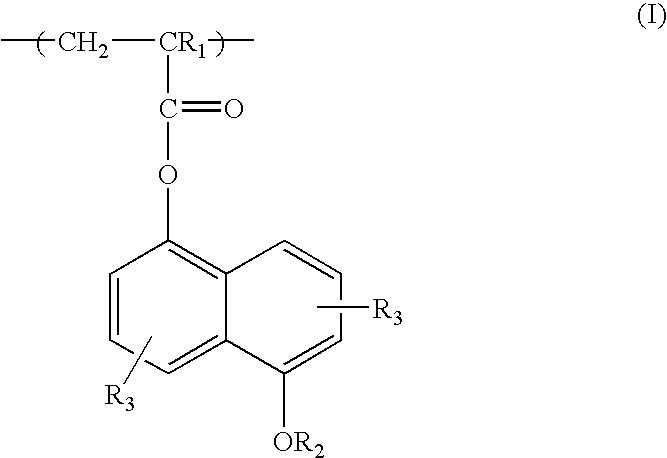
[0051] 5-hydroxy-1-naphthalenyl methacrylate (a.k.a. hydroxynaphthalene methacrylate or NAMA) monomer (2.60 g, 0.0045 mole), hexafluoroisopropyl methacrylate (iPrHFAMA) monomer (23.20 g, 0.0800 mole), 2-methacryloyl-gamma-butyrolactone (a.k.a. gamma-butyrolactone methacrylate or GBLMA) monomer (3.88 g, 0.0051 mole), azobisisobutyronitrile (AlBN) (0.91 g, 10% the total mole of all monomers), 150 g of tetrahydrofuran (THF) and 72 g of ethylacetate were added to a 250 ml 3-neck round bottom flask equipped with condenser, thermometer, nitrogen inlet and magnetic stirrer bar. The reaction mixture was stirred at room temperature and bubbled with N2 flow for 45 minutes after which is was heated to 67-70° C. and stirred for 14 hours with a blanket N2 flow. After reaction, the solution was then cooled to room temperature and added dropwise to 1200 g of hexane. The resulting slurry was stirred for two hours before filtration. S...
example 2
[0053] A terpolymer of ethylvinylether naphthalene methacrylate (NAMA-EVE) GBLMA, and iPrHFAMA with composition mole ratio of Oct. 20, 1970 was dissolved in PGMEA with 5 wt % BNBS-PFOS (based on the total weight of imaging polymer in the composition) and 0.18 wt % 1-t-butyloxycarbonyl 2-phenylbenzimidazole (based on the total weight of imaging polymer in the composition) to make a solution of 10% solid content. The resulting solution was filtered through a 0.2 μm filter. The resist was spin coated on a 8 inch silicon wafer which had a 900 Angstrom thick coating of Shipley's AR40 antireflective coating. The resist was post-apply baked (PAB) at 110° C. for 60 seconds and exposed to 193 nm wavelength light on a ASML 193 nm scanner (0.75 NA) using an alternative phase shift mask (Alt-PSM). The wafer was then developed without post-exposure bake (PEB) using a single-spray puddle develop process for 60 seconds with 0.263 N tetramethyl ammonium hydroxide (TMAH) developer. At dose of 8 mj / c...
PUM
 Abstract
Description
Claims
Application Information
 - R&D
- Intellectual Property
- Life Sciences
- Materials
- Tech Scout
- Unparalleled Data Quality
- Higher Quality Content
- 60% Fewer Hallucinations
Browse by: Latest US Patents, China's latest patents, Technical Efficacy Thesaurus, Application Domain, Technology Topic, Popular Technical Reports.
© 2025 PatSnap. All rights reserved.Legal|Privacy policy|Modern Slavery Act Transparency Statement|Sitemap|About US| Contact US: help@patsnap.com


