
Release layer paste and method of production of multilayer type electronic device

Inactive Publication Date: 2006-02-16
TDK CORPARATION
View PDF3 Cites 9 Cited by
  • Summary
  • Abstract
  • Description
  • Claims
  • Application Information

AI Technical Summary

Benefits of technology

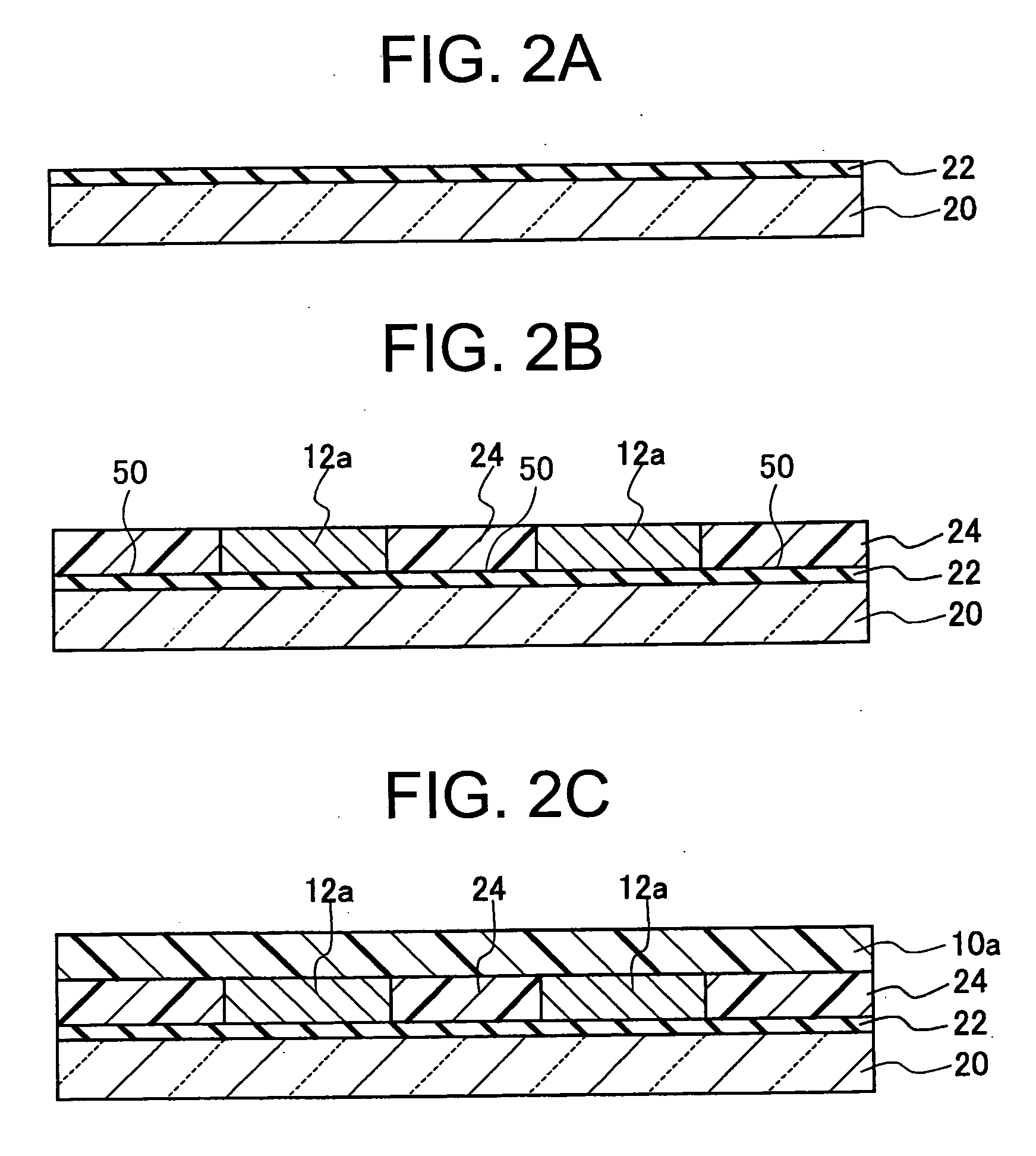
[0013] An object of the present invention is to provide a release layer paste used for producing a-multilayer type electronic device which does not cause sheet attack on an electrode layer paste for forming an electrode layer (if necessary, further a blank pattern layer paste for forming a blank pattern layer) and which enables formation of a release layer free of ablation at the time of printing of the paste and a method of production of a multilayer type electronic device using the release layer paste.
[0029] The release layer paste of the present invention is a paste comprised of a binder in which a specific acryl resin is contained as a main ingredient. The specific acryl resin contained in the paste in the present invention is hard to be dissolved or swelled by (is hardly soluble with) the terpineol, dehydroterpineol, terpineol acetate, or dehydroterpineol acetate contained as a solvent in electrode layer paste or blank pattern layer paste for forming the electrode layer or blank pattern layer. Therefore, there is the effect that the release layer formed using the release layer paste of the present invention is not subject to sheet attack by the electrode layer paste or blank pattern layer paste. As a result, the printability of the electrode layer paste or blank pattern layer paste for forming the electrode layer or blank pattern layer on the release layer formed using the release layer paste of the present invention is stable. Specifically, bleedout, shedding, and pinholes at the electrode layer or blank pattern layer formed on the surface of the release layer can be suppressed. Bleedout, shedding, and pinholes of the electrode layer and blank pattern layer easily occur due to the exposure of the supporting sheet due to dissolution of the release layer, but the release layer formed using the release layer paste of the present invention is not subject to sheet attack by the electrode layer paste or blank pattern layer paste, so the electrode layer or blank pattern layer itself will not crack due to dissolution and even if printed, will not shed residue etc. No bleedout, shedding, and pinholes of the electrode layer and blank pattern layer formed on the surface of the release layer will occur.
[0031] Further, the release layer formed using the release layer paste of the present invention is not ablated and does not generate residue at the time of printing of the electrode layer paste or blank pattern layer paste. Therefore, occurrence of defects (structural defects) at the time of stacking is suppressed and short-circuit defects of the finally obtained multilayer ceramic capacitor or other multilayer type electronic device can be reduced.
[0032] In the present invention, preferably the peeling strength of the first supporting sheet is controlled to 7.3 to 20.3 mN / cm (however, excluding 7.3 mN / cm and 20.3 mN / cm), whereby even if used combined with an electrode layer paste using terpineol, dehydroterpineol, terpineol acetate, or dehydroterpineol acetate as a solvent, the release layer formed using the release layer paste of the present invention will not drop off from the first supporting sheet.

Problems solved by technology

In the process of production of such electronic devices, the thicknesses of the green sheets able to form the dielectric layers after firing have become extremely thin (usually 1.5 μm or less), so at the time of formation of the electrode layers by the printing method, the solvent of the electrode layer paste causes the green sheets to dissolve, that is, the so-called “sheet attack” phenomenon becomes a problem.
This sheet attack phenomenon leads directly to defects of the green sheets and short-circuit defects, so is a problem which absolutely must be solved for making the layers thinner.
However, Japanese Patent Publication (A) No. 63-51616, Japanese Patent Publication (A) No. 3-250612, and Japanese Patent Publication (A) No. 7-312326 had the problem of a difficulty of peeling off the predetermined pattern of the electrode layer from the supporting film.
However, if using an electrode layer paste using terpineol or dehydroterpineol as a solvent together with a release layer using a butyral resin as a binder, the solvent of the electrode layer paste causes sheet attack at the release layer.
Sheet attack of the release layer becomes a cause of bleedout, shedding, and pinholes at the electrode layer or blank pattern layer formed on the surface of the release layer.
Further, the ablation of the release layer causes defects (structural defects) at the time of stacking and in turn can increase the short-circuit defects of the final multilayer type electronic device.

Method used


Image

  • Release layer paste and method of production of multilayer type electronic device
  • Release layer paste and method of production of multilayer type electronic device
  • Release layer paste and method of production of multilayer type electronic device

Examples


example 1

[0150] Preparation of Release Layer Paste

[0151] Preparation of Additive Slurry

[0152] First, as the additive (subcomponent) materials, (Ba, Ca) SiO3 in an amount of 1.48 parts by weight, Y2O3 in 1.01 parts by weight, MgCO3 in 0.72 part by weight, MnO in 0.13 part by weight, and V2O5 in 0.045 part by weight were prepared. Next, the prepared additive (subcomponent) materials were mixed to obtain the additive (subcomponent) material mixture.

[0153] Next, the additive material mixture in an amount of 4.38 parts by weight was mixed and pulverized with ethyl acetate in 13.9 parts by weight using a ball mill to obtain an additive slurry. The mixing and pulverization were performed using a 250 cc polyethylene resin vessel charged with 450 g of 2 mmφ ZrO2 media at a peripheral speed of 45 m / min for 20 hours. The pulverized additive material had a particle size of a median size of about 0.1 μm.

[0154] Preparation of Primary Slurry

[0155] Next, the entire amount of the obtained additive slurr...

example 2

[0189] The same procedure was performed as in Example 1 to prepare a release layer paste except for changing the acid value of the acryl resin as shown in Table 1. The results were similarly evaluated (Samples 1, 2, 4, and 5). The results are shown in Table 1.

TABLE 1Acryl acid valueElectrodelayer andCeramicAmountAmount ofPETblank patternpowderof resinplasticizerAcidpeelingElectrodelayer peelingSurfaceSam-(parts by(parts by(parts byvaluestrengthSheetPrint-Sheetprintingstrengthroughnesspleweight)weight)weight)P / B(mgKOH / g)(mN / cm)attackabilityresiduestate(mN / cm)Ra(μm)1Comp.10050251.33010.5GGPP13.30.112Ex.2Ex.10050251.33110.5GGGG14.40.083Ex.10050251.33510.5GGGG15.90.0774Ex.10050251.331010.5GGGG170.0785Comp.10050251.331510.5GGPP23.10.110Ex.

[0190] As shown in Table 1, when the acid value was 0 mgKOH / g, the surface roughness increases. Further, when the acid value was 15 mgKOH / g, the peeling strength and surface roughness of the electrode layer increased. As opposed to this, it could be c...

example 3

[0191] The same procedure was performed as in Example 1 to prepare a release layer paste except for changing the contents of the acryl resin and the plasticizer (parts by weight) with respect to 100 parts by weight of ceramic powder so as to change the content of acryl resin (parts by weight) with respect to 100 parts by weight of ceramic powder and the ratio (P / B) of the ceramic powder and, the acryl resin and plasticizer as shown in Table 2. The results were similarly evaluated (Samples 6 to 10). The results are shown in Table 2.

TABLE 2Electrodelayer andCeramicAmountAmount ofPETblank patternpowderof resinplasticizerAcidpeelingElectrodelayer peelingSurfaceSam-(parts by(parts by(parts byvaluestrengthSheetPrint-Sheetprintingstrengthroughnesspleweight)weight)weight)P / B(mgKOH / g)(mN / cm)attackabilityresiduestate(mN / cm)Ra(μm)6Comp.1006311.11510.5P*PPP10.90.097Ex.7Comp.1001265.56510.5P*PPP13.30.088Ex.8Ex.10024122.78510.5GGGG12.80.0793Ex.10050251.33510.5GGGG15.90.0779Comp.100100500.67510....


PUM

PropertyMeasurementUnit
Percent by massaaaaaaaaaa

Abstract

A release layer paste used for producing a multilayer type electronic device, used in combination with an electrode layer paste including terpineol, dehydroterpineol, terpineol acetate, or dehydroterpineol acetate and including a ceramic powder, organic vehicle, plasticizer, and dispersion agent, the organic vehicle containing a binder having an acryl resin as its main ingredient, the acryl resin being comprised of a copolymer having acrylic acid ester monomer units and methacrylic acid ester monomer units as its main ingredients and having an acid value of 1 to 10 mgKOH / g, a ratio (P / B) of the ceramic powder and the binder and plasticizer being controlled to 0.67 to 5.56 (however, excluding 0.67 and 5.56).

Description

BACKGROUND OF THE INVENTION [0001] 1. Field of the Invention [0002] The present invention relates to release layer paste used for production of a multilayer ceramic capacitor or other multilayer type electronic device and a method of production of a multilayer type electronic device using the release layer paste. [0003] 2. Description of the Related Art [0004] In recent years, due to the increasingly smaller sizes of electronic apparatuses, multilayer ceramic capacitors and other multilayer type electronic devices have become increasingly compact in size and sophisticated in performance. The thicknesses of the interlayer dielectric layers of multilayer type electronic devices (dielectric layers sandwiched between pairs of internal electrodes) have become 1 μm or less—enabling over 800 stacked layers. In the process of production of such electronic devices, the thicknesses of the green sheets able to form the dielectric layers after firing have become extremely thin (usually 1.5 μm o...

Claims


Application Information

Patent Timeline
IPC IPC(8): C03B29/00B32B18/00
CPCC04B35/4682Y10T428/252C04B35/62625C04B35/6264C04B35/62665C04B35/63C04B35/632C04B35/63424C04B2235/3206C04B2235/3215C04B2235/3225C04B2235/3239C04B2235/3262C04B2235/3436C04B2235/3454C04B2235/5436C04B2235/5445C04B2235/6582C04B2235/96H01G4/308H05K1/0306H05K3/207H05K3/4611H05K3/4629H05K2201/09881H05K2203/0156C04B35/6261H01G4/30
Inventor ISHIYAMA, TAMOTSUSATO, SHIGEKI
Owner TDK CORPARATION
Learn More