Information recording medium and process for producing the same
a technology of information recording and information, applied in the field of optical information recording medium, can solve the problems of difficult control of the size and edge of a minute recorded mark formed on the recording layer with a high density recording, and the inability of conventional write-once-read-many optical discs to fully realize the characteristics of optical discs, and achieve excellent reproduction properties
- Summary
- Abstract
- Description
- Claims
- Application Information
AI Technical Summary
Benefits of technology
Problems solved by technology
Method used
Image
Examples
example 1
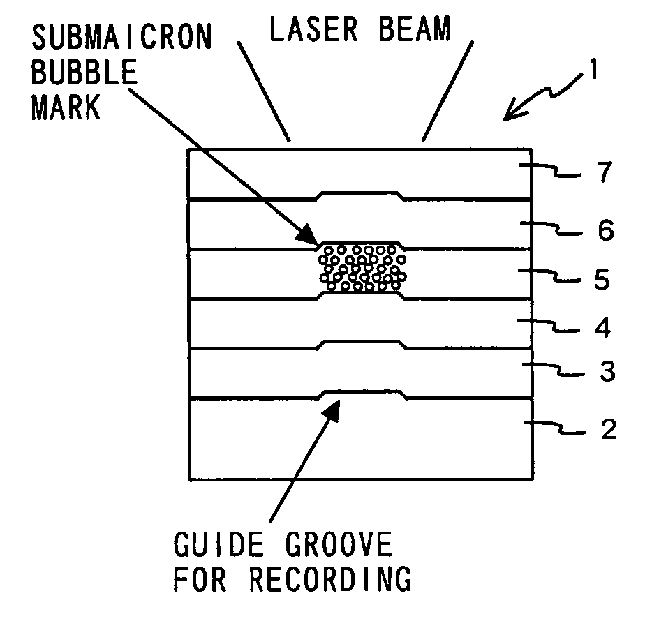
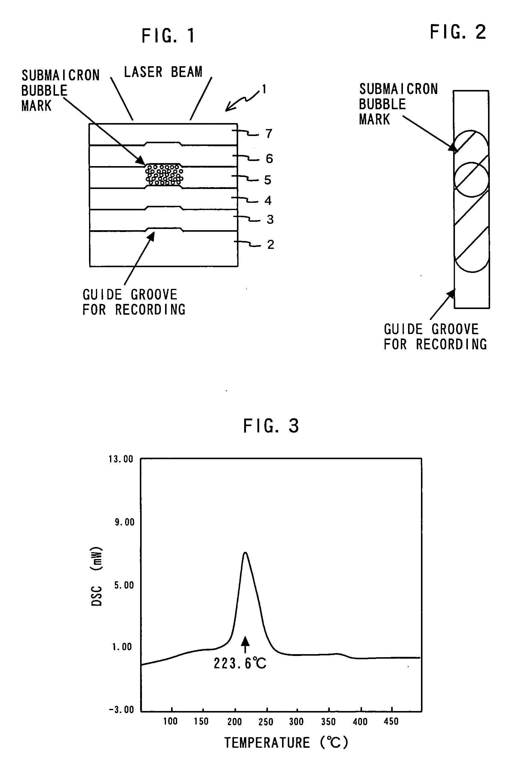
[0059] A reflecting layer 3, a first dielectric layer 4, a recording layer 5, a second dielectric layer 6, and a light transparent covering layer 7 were formed in turn on the surface of a substrate 2 to make a sample of an optical disc as Example 1 which has a configuration shown in FIG. 1.
[0060] As a light reflecting side substrate, there was used a substrate having a thickness of 1.1 mm and a diameter of 12 cm made of polycarbonate resin on which a spiral groove having a 27 nm depth and a pitch of 0.320 mm was provided.
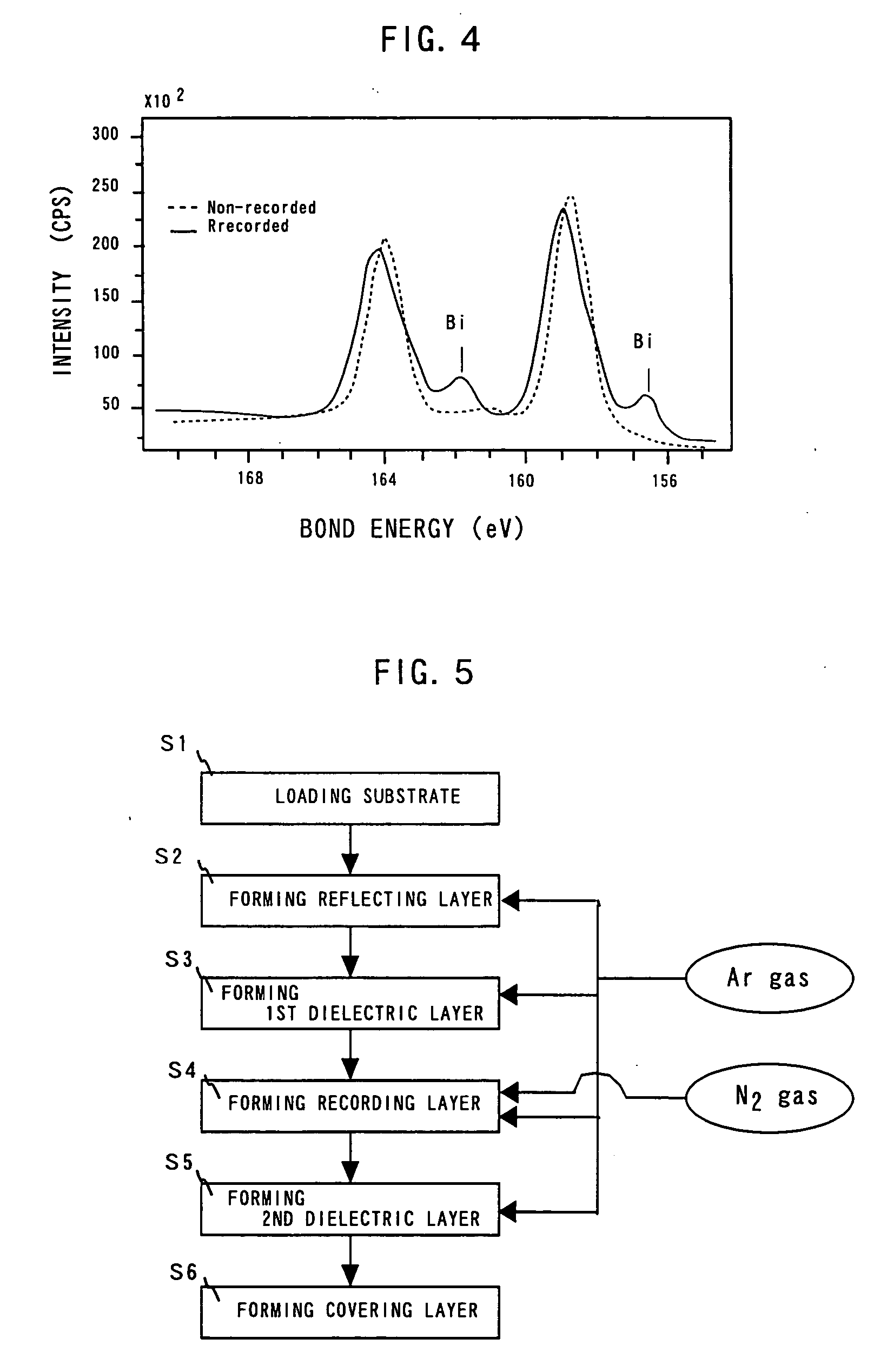
[0061] A reflecting layer of Ag—Pd—Cu alloy having a thickness of 100 nm, and a first dielectric layer of ZnS—SiO2 having a thickness of 10 nm were sequentially deposited on the substrate by a sputtering method.
[0062] Subsequently, a recording layer having a thickness of 12 nm was deposited in an atmosphere of 10 sccm of N2 gas with respect to 80 sccm of Ar gas by a reactive sputtering method using a Bi—Ge target. The condition during reactive sputtering is, for ...
example 2
[0066] An optical disc of Example 2 was formed in the same manner as Example 1 except that a recording layer was subjected to reactive sputtering and deposited in an atmosphere of 20 sccm of N2 gas with respect to 70 sccm of Ar gas to provide the second dielectric layer of ZnS—SiO2 having a thickness of 25 nm at the light incident side.
[0067] When a random pattern was recorded, and a jitter after recording was measured in the same manner as Example 1 except that a recording laser power of 5.0 mW was used in this Example, a satisfactory jitter of about 7.5% was obtained.
example 3
[0068] An optical disc of Example 3 was formed in the same manner as Example 1 except that a recording layer was subjected to reactive sputtering and deposited in an atmosphere of 40 sccm of N2 gas with respect to 50 sccm of Ar gas to provide the second dielectric layer of ZnS—SiO2 having a thickness of 20 nm.
[0069] When a random pattern was recorded, and a jitter after recording was measured in the same manner as Example 1 except that a recording laser power was 5.0 mW in this Example, a satisfactory jitter of about 7.3% was obtained.
PUM
| Property | Measurement | Unit |
|---|---|---|
| Temperature | aaaaa | aaaaa |
| Temperature | aaaaa | aaaaa |
| Fraction | aaaaa | aaaaa |
Abstract
Description
Claims
Application Information
 - R&D
- Intellectual Property
- Life Sciences
- Materials
- Tech Scout
- Unparalleled Data Quality
- Higher Quality Content
- 60% Fewer Hallucinations
Browse by: Latest US Patents, China's latest patents, Technical Efficacy Thesaurus, Application Domain, Technology Topic, Popular Technical Reports.
© 2025 PatSnap. All rights reserved.Legal|Privacy policy|Modern Slavery Act Transparency Statement|Sitemap|About US| Contact US: help@patsnap.com


