
Semiconductor storage device

a technology of semiconductors and storage devices, applied in semiconductor devices, electrical devices, transistors, etc., can solve the problems of difficult to scale down the film difficult to reduce the thickness of the gate, and increase the short channel effect, so as to achieve the effect of suppressing short channel effects, sufficient memory functions, and suppressing interference at the time of rewriting

Inactive Publication Date: 2005-10-13
SHARP KK
View PDF8 Cites 14 Cited by
  • Summary
  • Abstract
  • Description
  • Claims
  • Application Information

AI Technical Summary

Benefits of technology

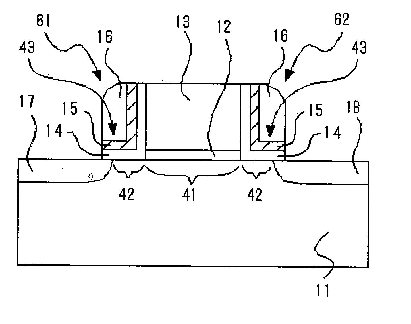
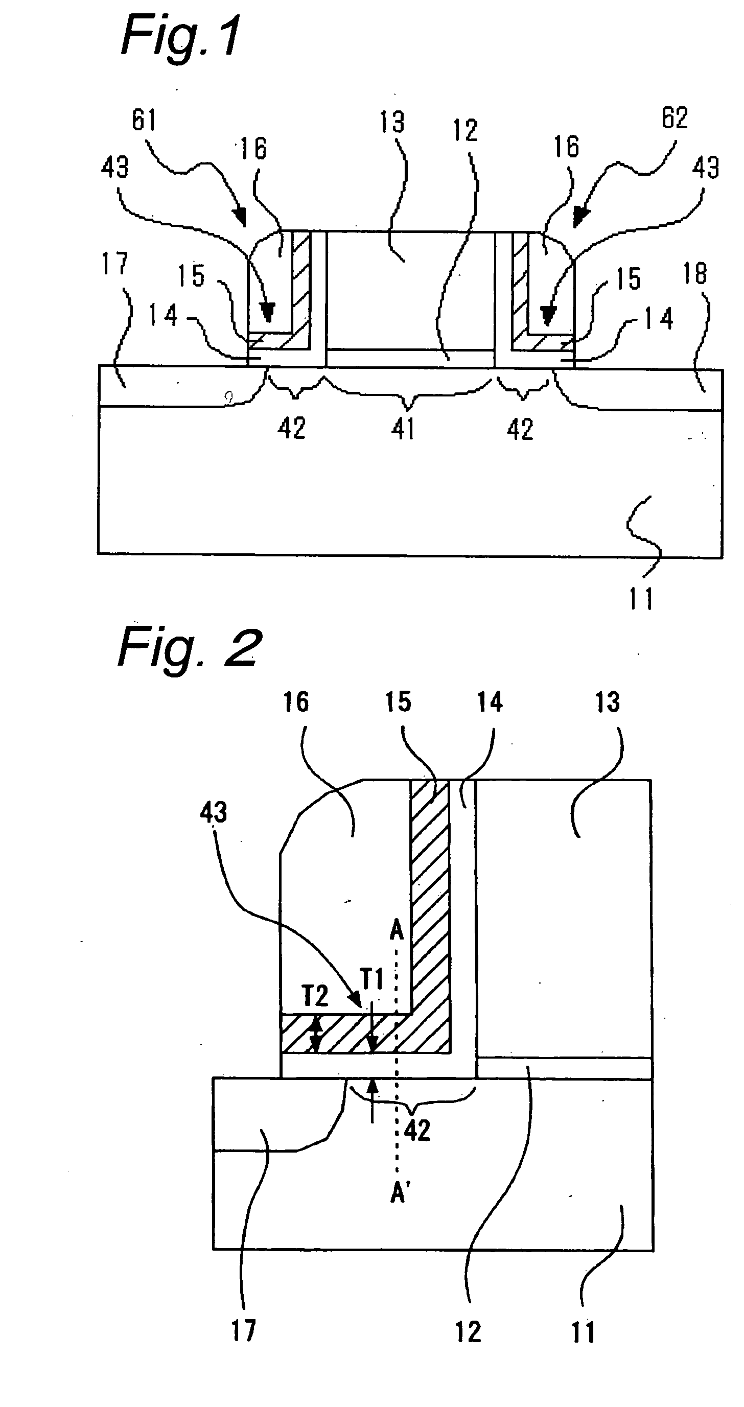
[0016] According to the semiconductor storage device of the constitution, two charge holding portions, formed on opposite sidewalls of the gate electrode, are independent of the gate insulating film so that the memory function carried out by the charge holding portions and the transistor operation function carried out by the gate insulating film are separated. Therefore, it is easy to form the gate insulating film as a thin film so that short channel effects are suppressed while retaining a sufficient memory function. In addition, the two charge holding portions, formed on opposite sides of the gate electrode, are separated by the gate electrode and, therefore, interference at the time of rewriting can be effectively suppressed. In other words, the distance between the two charge holding portions can be reduced. Accordingly, a semiconductor storage device wherein two bit operation is possible and miniaturization is easy can be provided.
[0058] According to the semiconductor device of the above embodiment, the film made of the first insulator having the function of charge storage includes a portion extending approximately parallel to the sides of the gate electrode and, therefore, the amount of charge injected to the film made of the first insulator having the function of charge storage increases at the time of the rewrite operation and, thereby, the rewrite speed is increased.

Problems solved by technology

In the memory, however, a gate insulating film has a three-layered ONO film structure, which is difficult to form as a thin film, and a problem arises wherein miniaturization of elements is difficult.
That is to say, it is difficult to scale down the film thickness of the gate insulating film and, therefore, short channel effects are increased and miniaturization of elements cannot be achieved.
In addition, as channel length decreases, it becomes difficult to separate the two charge holding portions 907 and 908 in one transistor and, therefore, further miniaturization of elements cannot be achieved.

Method used


Image

  • Semiconductor storage device
  • Semiconductor storage device
  • Semiconductor storage device

Examples


embodiment 1

[0108] In a memory element forming a semiconductor storage device of the present embodiment as shown in FIG. 1, a gate electrode 13 having a gate length of approximately the same length as a conventional transistor, for example from approximately 0.015 μm to 0.5 μm, is formed above a semiconductor substrate 11 via a gate insulating film 12 and charge holding portions 61 and 62 in the form of sidewall spacers are formed on the gate insulating film 12 and on the sidewalls of gate electrode 13 so as to form a non-volatile memory cell that allows the storage of two bits. In addition, first and second diffusion layer regions 17 and 18 (source / drain regions) are formed on the side of charge holding portions 61 and 62 opposite to gate electrode 13 wherein these charge holding portions 17 and 18 are offset relative to the edges of gate electrode 13 (offset from region 41 on which gate electrode 13 is formed).

[0109] As described above, charge holding portions 61 and 62 of the memory transis...

embodiment 2

[0148] A memory element, which is a semiconductor storage device of the present Embodiment 2, is provided by restricting charge injection into charge holding portions from the gate electrode in the semiconductor storage device according to the above Embodiment 1.

[0149] The memory element of the present embodiment is described in reference to FIG. 8 below. The memory element of the present embodiment is characterized in that thickness T1B of silicon oxide film 14 on a sidewall of gate electrode 13 is greater than thickness T1A of silicon oxide film 14 on semiconductor substrate 11. Therefore, charge injection from gate electrode 13 to silicon nitride film 15 (or charge release from silicon nitride film 15 to gate electrode 13) can be effectively restricted. Accordingly, the rewriting characteristics of the memory element become stable and the reliability is increased.

[0150] The procedure for the formation of the memory element of the present Embodiment 2 is described in reference t...

embodiment 3

[0152] In the semiconductor storage device of the present Embodiment 3, charge holding portions 161 and 162 are formed of regions for charge storage (may be regions for storing charges or films having a function of charge storage) and of regions for preventing charges from escaping (may be films having a function of preventing charges from escaping), as shown in FIG. 10. The semiconductor storage device has, for example, ONO structure. That is to say, silicon nitride film 142, as an example of a film made of a first insulator, is sandwiched between silicon oxide film 141, as an example of a film made of a second insulator, and silicon oxide film 143, as an example of a film made of a third insulator so as to form charge holding portions 161 and 162. Here, silicon nitride film 142 has a function of charge storage. In addition, silicon oxide films 141 and 143 act as films having the function of preventing the escape of charges stored in the silicon nitride film 142.

[0153] In addition...


PUM


Abstract

A semiconductor storage device wherein storage of two bits is implemented in one transistor and that can be further minaturized is provided. Two charge holding portions, one on each sidewall of the gate electrode, are formed so as to be independent of the gate insulating film. Thereby, the memory function carried out by the charge holding portions and the transistor operation function carried out by the gate insulating film are separated. The two charge holding portions, formed on opposite sides of the gate electrode, are separated by the gate electrode and, therefore, interference at the time of rewriting can be effectively suppressed. Accordingly, a semiconductor storage device wherein storage of two bits is implemented in one transistor and that is minaturized is provided.

Description

TECHNICAL FIELD [0001] The present invention relates to a semiconductor storage device, in particular, to a semiconductor storage device composed of a field effect transistor having a function to convert the change of an electric charge to the amount of electric current. BACKGROUND ART [0002] There is a memory according to a prior art developed by Saifun Semi conductors Ltd. as a non-volatile memory wherein one field effect transistor allows the storage of two bits (Kohyo (Japanese Unexamined Publication) No.2001-512290). [0003] This memory is configured of a gate electrode 909 formed above a P type well region 901 via a gate insulating film as well as of first and second N type diffusion layer regions 902 and 903 formed in the surface of P type well region 901. The gate insulating film is a so-called ONO (Oxide Nitride Oxide) film wherein a silicon nitride film 906 is sandwiched between silicon oxide films 904 and 905. Charge holding portions 907 and 908, respectively, are formed i...

Claims


Application Information

Patent Timeline
Patent Type & Authority Applications(United States)
IPC IPC(8): H01L21/8247H01L27/115H01L29/788H01L29/792
CPCH01L29/7923H01L29/4234H01L29/7887
Inventor IWATA, HIROSHISHIBATA, AKIHIDE
Owner SHARP KK
Learn More