System and Method for the Identification of Chemical Mechanical Planarization Defects

a technology of mechanical planarization and system and method, applied in the direction of manufacturing tools, lapping machines, instruments, etc., can solve the problems of significant loss in productivity, significant loss from the standpoint of material cost, labor and productivity, and achieve the effect of reducing quality loss, increasing productivity, and reducing the need for expensive metrology

Inactive Publication Date: 2005-10-13
UNIV OF SOUTH FLORIDA
View PDF12 Cites 8 Cited by
  • Summary
  • Abstract
  • Description
  • Claims
  • Application Information

AI Technical Summary

Benefits of technology

[0018] As such, the present invention presents a novel application of a wavelet-based multiscale method in a nanomachining process chemical mechanical planarization (CMP) of wafer fabrication. The application involves identification of delamination defects of low-k dielectric layers by analyzing the nonstationary acoustic emission (AE) signal signal collected during copper damascene (Cu-low k) CMP process. An offline strategy and a moving window-based strategy for online implementation of the wavelet monitoring approach are provided. The results show that the wavelet-based approach using the AE signal offers an efficient means for real-time detection of delamination defects in CMP processes. Such an online strategy, in contrast to the existing offline approaches, offers a viable tool for CMP process control.
[0019] The present invention detects delamination during the fabrication process, through analysis of online sensor data. The wavelet based multiresolution analysis method in accordance with the present invention is used in the process of sensor data analysis. The present invention benefits the semiconductor manufacturing industry by reducing quality losses, increasing productivity, reducing the need for expensive metrology and reducing the dependence and cost of final inspection of the wafers.

Problems solved by technology

Delamination is a commonly occurring defect in the wafer fabrication process, which causes significant loss in productivity.
Since such defects are only visible under a powerful microscope, such as a Scanning Electron Microscope (SEM), often these defects are not detected until the final testing phase of the wafer circuitry, thus resulting in significant losses from the standpoint of material costs, labor and productivity.

Method used


Image

  • System and Method for the Identification of Chemical Mechanical Planarization Defects
  • System and Method for the Identification of Chemical Mechanical Planarization Defects
  • System and Method for the Identification of Chemical Mechanical Planarization Defects

Examples


Embodiment Construction

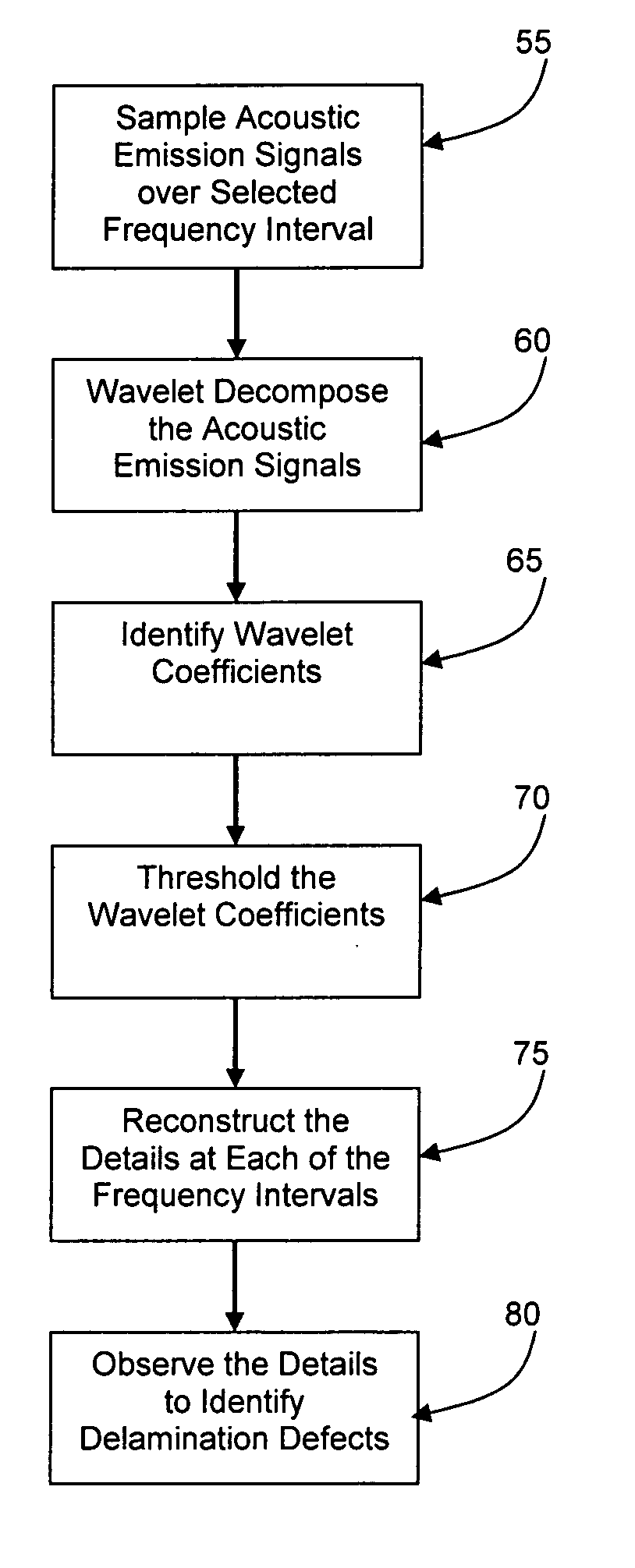
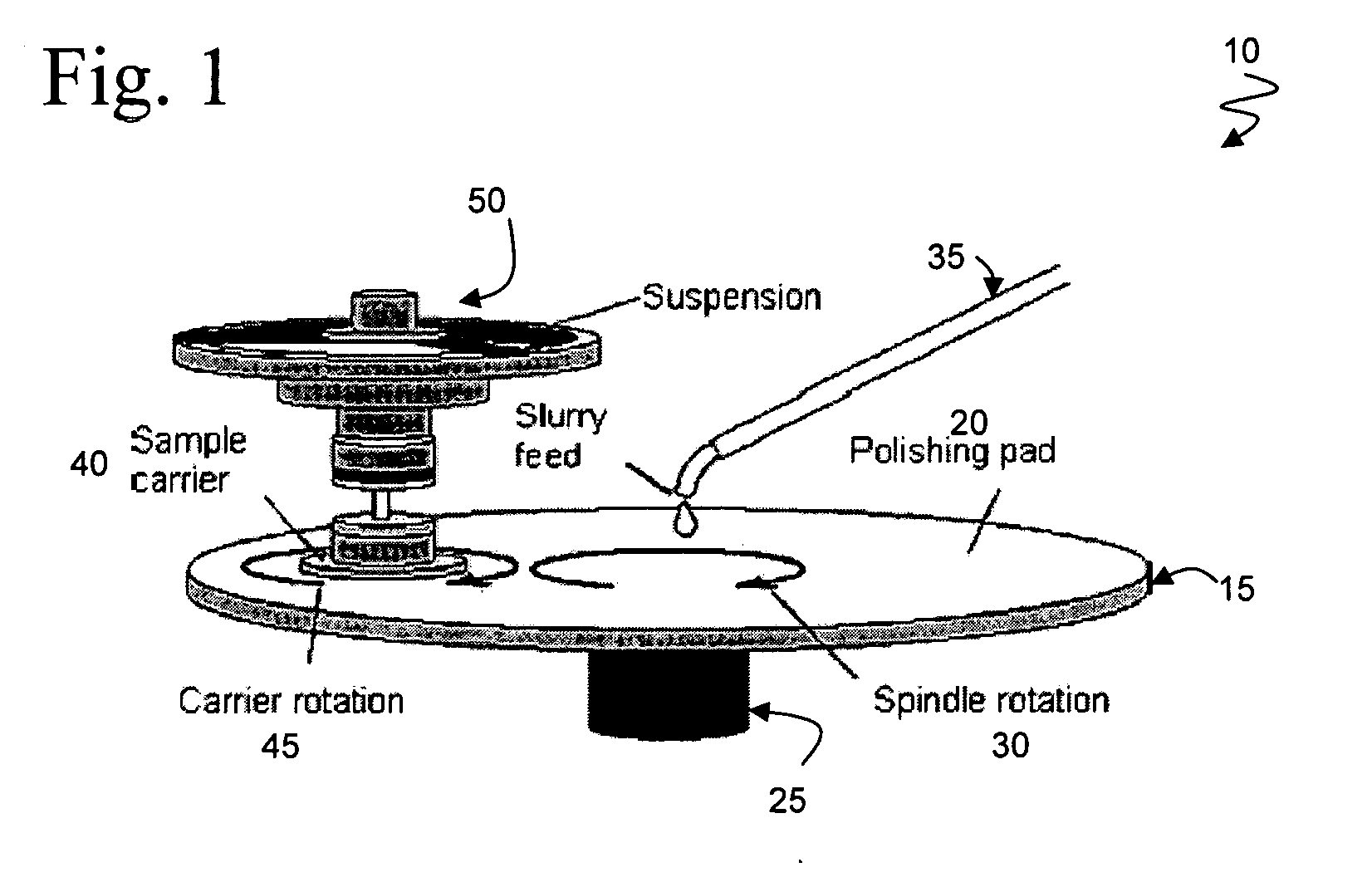
[0032] The chemical mechanical planarization process has been made more challenging in recent years due to the complex wafer topographies and the introduction of copper (instead of aluminum) and low-k dielectrics. The multilevel metallization process typically consists of etching, deposition, and planarization using a copper Damascene process. FIG. 1 illustrates a CMP setup in accordance with the present invention, which synergistically combines both tribological (abrasion) and chemical (etching) effects to achieve planarization. With reference to FIG. 1, the wafer polisher 10 includes a polishing platen 15 to which a polishing pad 20 is affixed. Polishing platen 15 includes a connection 25 to a drive mechanism (not shown) which enables the platen 15 and pad 20 to be rotated in at least one rotational direction 30. A conduit 35 dispenses a polishing slurry, typically silica or alumina abrasive particles suspended in either a basic or an acidic solution, onto polishing pad 20.

[0033]...


PUM


Abstract

The present invention presents a novel application of a wavelet-based multiscale method in a nanomachining process chemical mechanical planarization (CMP) of wafer fabrication. The invention involves identification of delamination defects of low-k dielectric layers by analyzing the nonstationary acoustic emission (AE) signal collected during copper damascene (Cu-low k) CMP processes. An offline strategy and a moving window-based strategy for online implementation of the wavelet monitoring approach are developed.

Description

CROSS-REFERENCE TO RELATED APPLICATION [0001] This application claims priority to U.S. Provisional Patent Application No. 60 / 521,357, entitled: “Method of Identifying Defects in Chemical Mechanical Planarization”, filed Apr. 8, 2004.BACKGROUND OF INVENTION [0002] Some of the critical requirements facing semiconductor device manufacturing are continual feature-size reduction, introduction of new materials for higher processing speeds and improved reliability, multilevel metallization (MLM), or interconnections, and increased productivity through larger wafer sizes. Wafer polishing using chemical mechanical planarization (CMP) is a key nanoscale manufacturing step that can significantly impact how the above requirements are met by the industry. However, the increased sophistication of the CMP process has brought difficult manufacturing challenges including the identification of defects such as delamination, dishing, under / over polishing, process monitoring, and process control. [0003]...

Claims


Application Information

Patent Timeline
IPC IPC(8): B24B37/005B24B49/00G01N29/00G01N29/04G01N29/12G01N29/14G01N29/34G01N29/42G01N29/44G01N29/46
CPCB24B37/005B24B49/003G01N29/043G01N29/12G01N29/14G01N29/348G01N29/42G01N29/4427G01N29/4445G01N29/46G01N2291/0231G01N2291/2632G01N2291/2697
Inventor GANESAN, RAJESHDAS, TAPAS K.SIKDER, ARUN K.KUMAR, ASHOK
Owner UNIV OF SOUTH FLORIDA
Why Eureka
Try Eureka