Single crystal material having high density dislocations arranged one-dimensionally in straight line form, functional device using said single crystal material, and method for their preparation

a single crystal material and high density technology, applied in the field of ceramic or metal single crystal material having high density dislocations arranged one-dimensionally on respective straight lines, a functional device, can solve the problem of limited utilization of the dislocation mechanism

Inactive Publication Date: 2005-10-06
JAPAN SCI & TECH CORP
View PDF0 Cites 0 Cited by
  • Summary
  • Abstract
  • Description
  • Claims
  • Application Information

AI Technical Summary

Benefits of technology

[0007] Secondly, the present invention provides a device for high-speed dislocation-pipe diffusion of ions or electron, comprising the above single-crystal material.
[0008] Thirdly, the present invention provides a quantum wire device comprising a single-crystal material made of ceramic or metal, which has dislocations arranged one-dimensionally on respective straight lines at a high density of 106 to 1014/cm2, and quantum wires consisting of metal atoms introduced in the single-crystal material through a diffusion treatment. The quantum wires are arranged along the corresponding dislocations at a high density of 106 to 1014/cm2.
[0009] Fourthly, the present invention provides a thin film device comprising a single-crystal thin film made of ceramic or metal, which internally has dislocations arranged one-dimensionally on respective straight lines at a high density of 106 to 1014/cm2, and nano-hole bundles formed along the corresponding dislocations.
[0010] Fifthly, the present invention provides -a method of producing a single-crystal material made of ceramic or metal, which internally has dislocations arranged one-dimensionally on respective straight lines at a high density of 106 to 1014/cm2. The method comprises compressing a single-crystal blank made of ceramic or metal, from a direction allowing the activation of a single slip, in a temperature range of a brittle-to-ductile transition temperature (BDTT) to about a melting point of the single-crystal blank to induce plastic deformation therein, and subjecting the resulting product to a heat treatment at a high temperature of one-half or more of the melting point by absolute temperature.
[0011] Sixthly, the present invention provides a ...

Problems solved by technology

However, in view of industrial application, the dislocation mechanism has been limi...

Method used


Image

  • Single crystal material having high density dislocations arranged one-dimensionally in straight line form, functional device using said single crystal material, and method for their preparation
  • Single crystal material having high density dislocations arranged one-dimensionally in straight line form, functional device using said single crystal material, and method for their preparation
  • Single crystal material having high density dislocations arranged one-dimensionally in straight line form, functional device using said single crystal material, and method for their preparation

Examples


example

(Example 1)

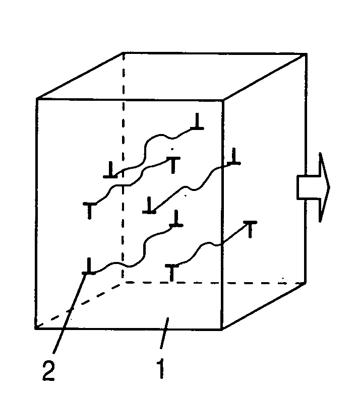
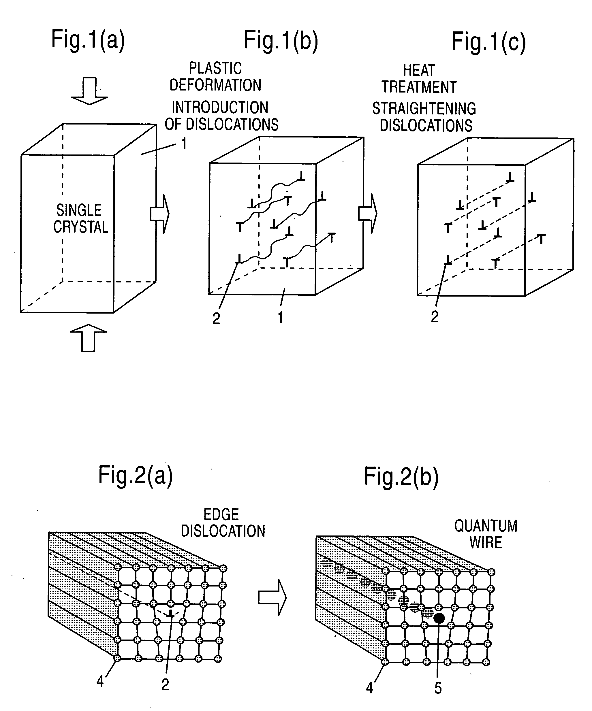
[0040] As schematically shown in FIG. 5(a), a cubic zirconia single-crystal sample of 5 mm (length)×5 mm (width)×10 mm (height) was compressed using an electrohydraulic compression machine under the conditions that a crosshead speed is a constant value of 0.005 mm / min, an angle between the normal line relative to the principal slip plane (001) face and the compression axis being 55 degree, an atmosphere being normal atmosphere and a temperature being 1300° C., to induce a plastic deformation of 1% (strainε=8.3×10⁶). A principal slip direction was [110], and a compression direction was [112]. Then, the sample was subjected to a heat treatment at 1300° C. for 1.5 hours. Edge dislocations introduced by the heat treatment after the compression are schematically shown in FIG. 5(b).

[0041] The zirconia single crystal having high-density dislocations introduced therein was polished. Then, the single crystal was subjected to an ion thinning process to have a reduced thickness, a...

example 2

(Example 2)

[0044] Under the same conditions as those of Example 1, except for using alumina single crystal (sapphire) as a single crystal sample, dislocations were formed in the sample, and titanium was deposited on the sample through a vacuum deposition process. Then, the deposited titanium was diffused at a temperature of 1400° C. and a pressure of 1 atom or less under an Ar gas atmosphere for 2 hours. FIG. 7(a) is an energy dispersive spectroscopic (EDS) image of the sample after the titanium deposition at a position just above a basal dislocation (circled zone B) and at a position away from the basal dislocation by 20 nm (circled zone A). FIG. 7(b) is an EDS spectrum obtained at a position of the circled zone A, and FIG. 7(c) is an EDS spectrum at a position just above one of the dislocations. The measurement was conducted using a probe with a diameter of 1 nm. As seen in FIG. 7(c), 3 to 5 at % of titanium exists at the position of the dislocation. This means that titanium atoms...


PUM


Abstract

Disclosed is a ceramic or metal single-crystal material having high-density dislocations arranged one-dimensionally on respective straight lines. The single-crystal material is produced by compressing a ceramic or metal single-crystal blank at a high temperature from a direction allowing the activation of a single slip to induce plastic deformation therein, and then subjecting the resulting product to a heat treatment. The single-crystal material can be used in a device for high-speed dislocation-pipe diffusion of ions or electrons. The single-crystal material can further be subjected to a diffusion treatment so as to diffuse a metal element from its surface along the dislocations to provide a single-crystal device with a specific electrical conductivity or a quantum wire device. Otherwise, the single-crystal material can be subjected to annealing or chemical etching so as to form nano-holes along the high-density dislocations to provide a thin film device, such as a molecular sieve film or a carbon-dioxide separating film.

Description

TECHNICAL FIELD [0001] The present invention relates to a ceramic or metal single-crystal material having high-density dislocations arranged one-dimensionally on respective straight lines, a functional device using the single-crystal material, and methods of producing them. BACKGROUND ART [0002] A solid material, such as ceramics or metals, includes a portion where micro-regions with a disordered atomic arrangement continuously align in a line. This portion is referred to as “dislocation”). The dislocation is classified broadly into “edge dislocation” and “screw dislocation”. These dislocations are formed, for example, during the course of solidification of a molten material or in conjunction with plastic deformation of a solid material. If the density of dislocations in a material is increased, the material can have an enhanced strength. [0003] A structure adapted to two-dimensionally confine electrons and allow only one-dimensional electron motion is known and described as a quant...

Claims


Application Information

Patent Timeline
IPC IPC(8): C30B29/16C30B1/12C30B29/20C30B33/00H01L29/06H01L29/32
CPCB82Y10/00B82Y30/00C30B1/12C30B33/00H01L29/32C30B29/16C30B29/20
Inventor IKUHARA, YUICHIYAMAMOTO, TAKAHISA
Owner JAPAN SCI & TECH CORP
Why Eureka
Try Eureka