
Low-k dielectric material system for IC application

a dielectric material and low-k technology, applied in the direction of electrical apparatus, semiconductor devices, semiconductor/solid-state device details, etc., can solve the problems of very different solubility of boron-rich networks and silicon dioxide networks, and achieve small marginal increase in total interconnect capacitance, high wiring level, and high strength

Inactive Publication Date: 2005-09-15
GLOBALFOUNDRIES U S INC
View PDF7 Cites 34 Cited by
  • Summary
  • Abstract
  • Description
  • Claims
  • Application Information

AI Technical Summary

Benefits of technology

The solution provides a low-dielectric constant interlayer dielectric material with high strength and reduced thermal stress, maintaining mechanical integrity and improving chip performance by minimizing signal delays and power consumption.

Problems solved by technology

The applicants however are unaware of any prior art that discloses that such CPG materials can be used as an ILD material for applications in semiconductor interconnect structures.
One key feature of CPG materials is that the solubility of the boron-rich network and the silicon dioxide network are very dissimilar.

Method used


Image

  • Low-k dielectric material system for IC application
  • Low-k dielectric material system for IC application
  • Low-k dielectric material system for IC application

Examples


Embodiment Construction

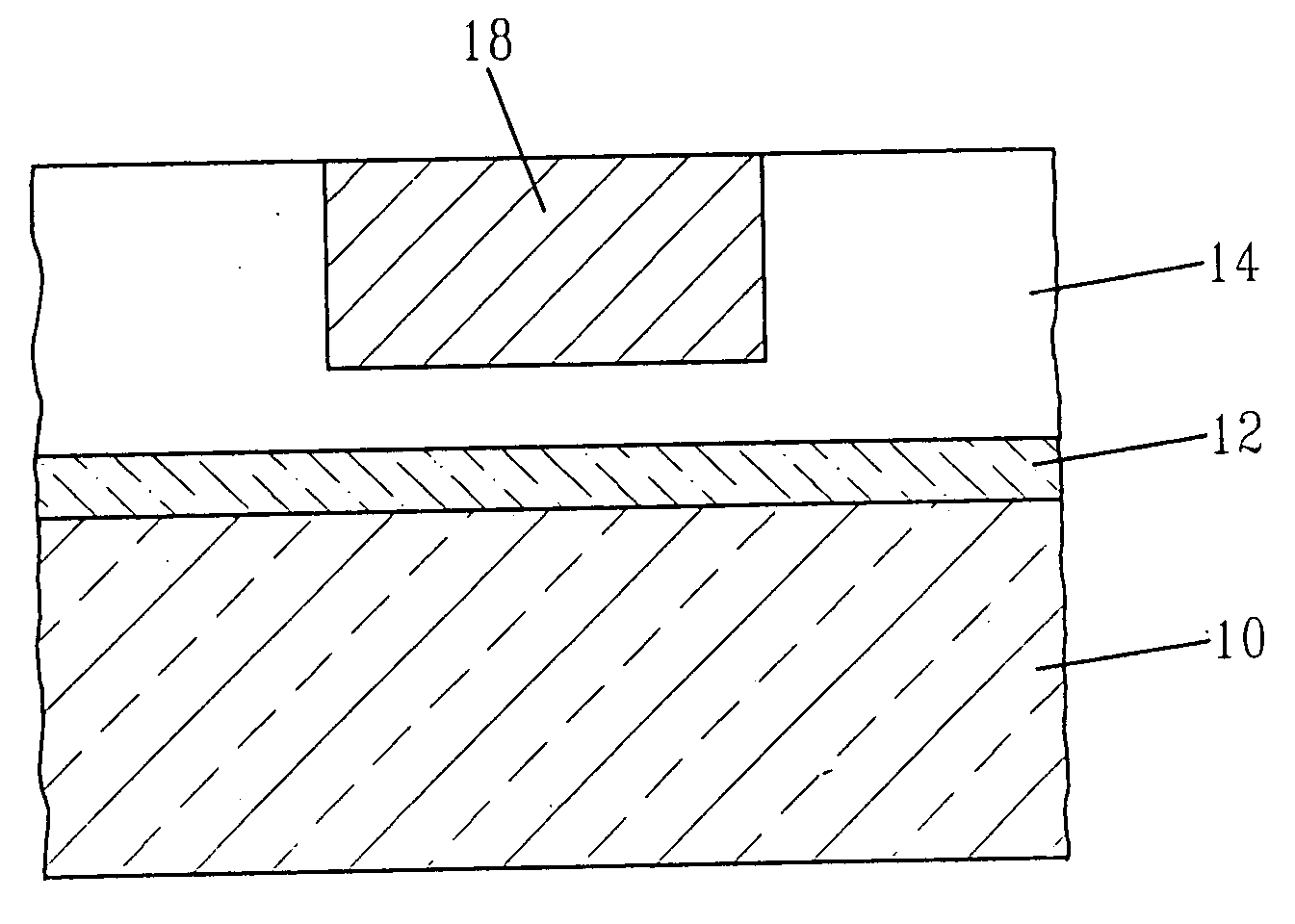
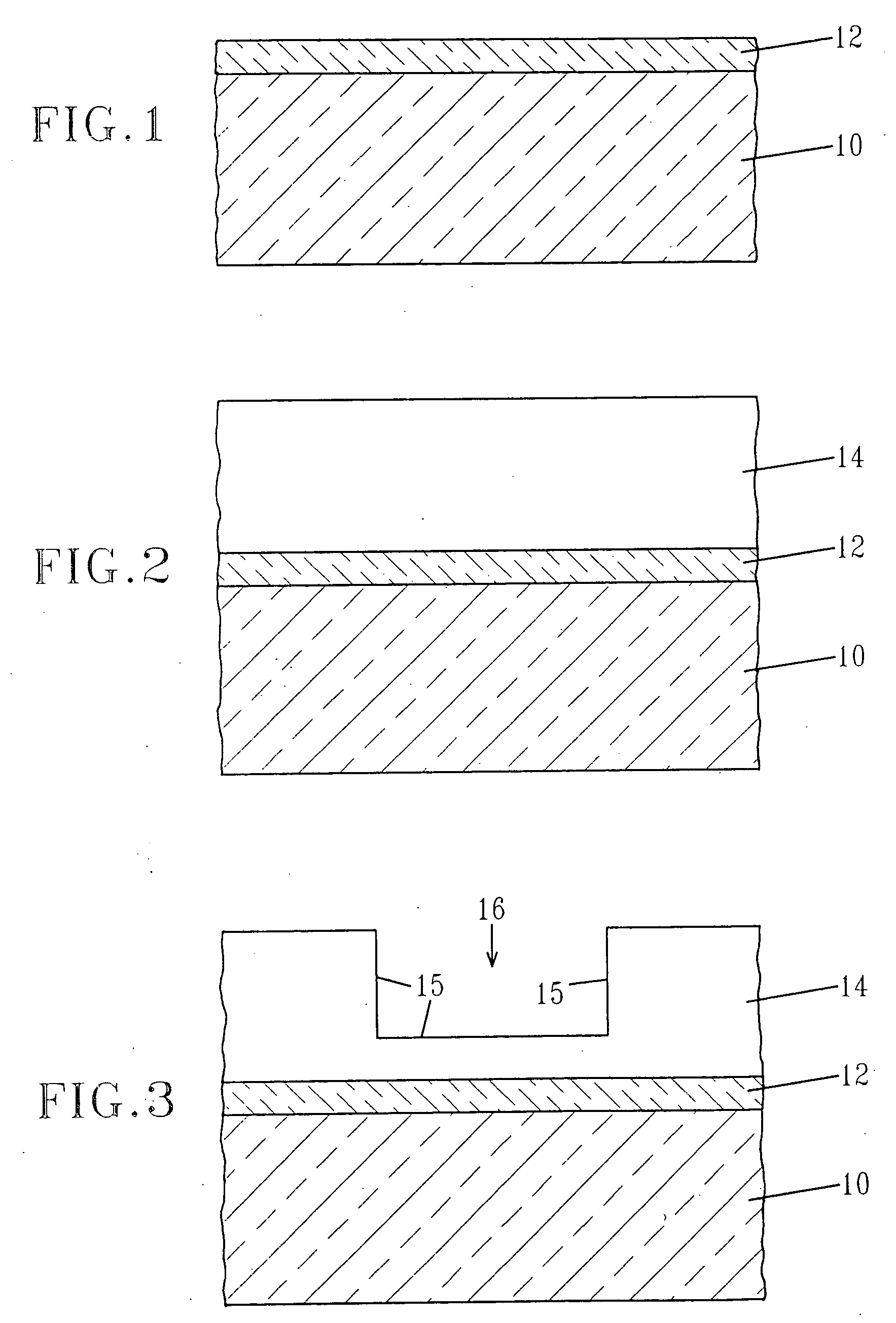
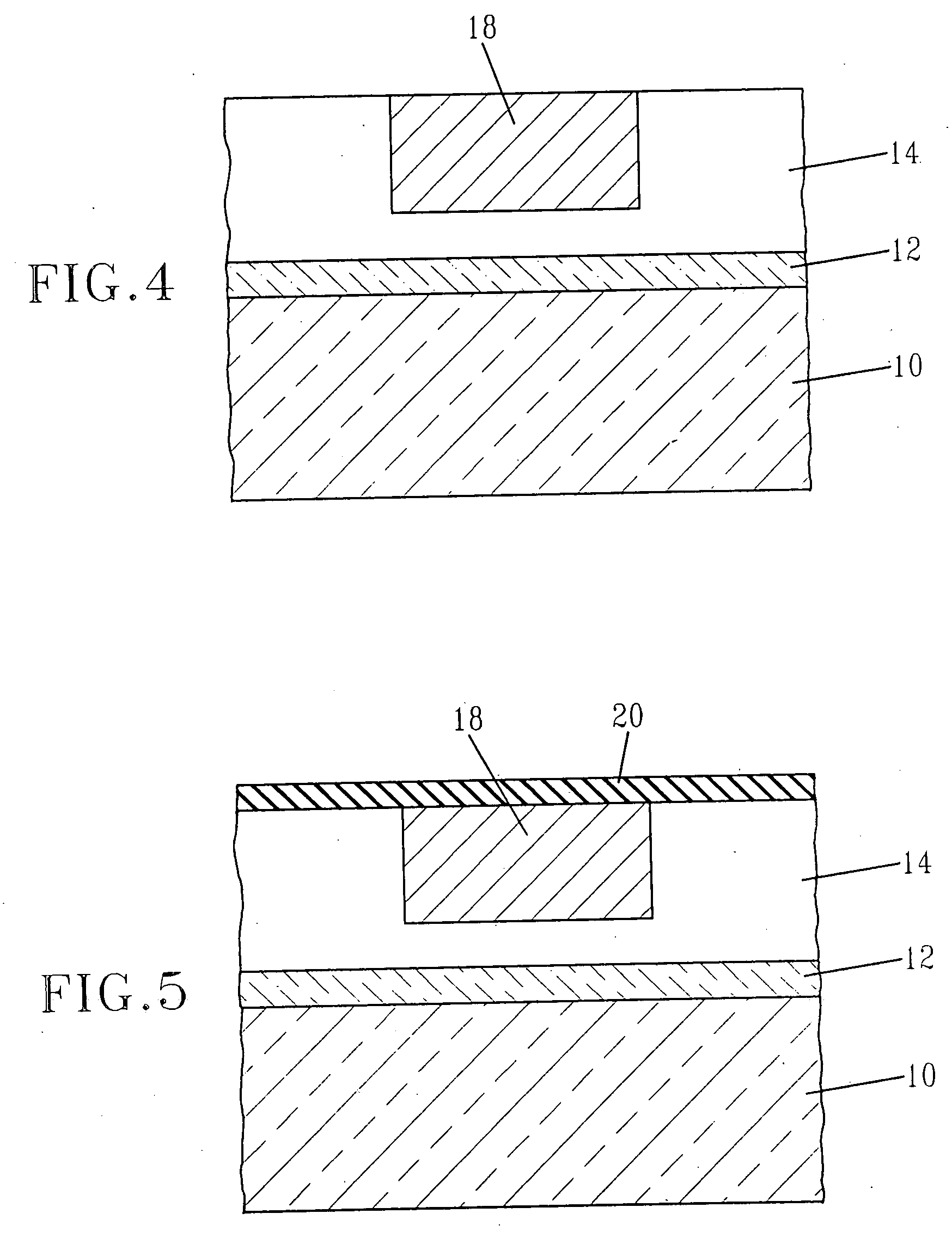
[0035] The present invention, which provides a new ILD material for use in semiconductor interconnect structures as well as a method of fabricating such interconnect structures, will now be described in greater detail by referring to the drawings that accompany the present application. It should be noted that the drawings of the present application are not drawn to scale. Moreover, although the drawings of the present invention show only a single metal wiring region within the ILD material, the present invention is not limited to such a structure. Instead, the ILD material of the present invention can contain many wiring regions therein and various wiring levels can be stacked one atop another. The various wiring levels can be interconnected by metal vias using technology well known to those skilled in the interconnect art. A single damascene or dual damascene process can be used in forming the interconnect structure.

[0036] Reference is first made to the initial structure that is s...


PUM

PropertyMeasurementUnit
dielectric constantaaaaaaaaaa
porosityaaaaaaaaaa
pore sizeaaaaaaaaaa

Abstract

A low-k dielectric for use as an interlayer for an interconnect structure is provided. The dielectric of the present invention is an alkaline boron silicate glass which when formulated in certain compositional ranges can undergo spinodal decomposition when processed using certain thermal profiles. Spinodal decomposition is a chemical and physical separation of the silicate glass into a distinct interpenetrating microstructure which contains a substantially pure silicon dioxide network and a boron-rich network. The dimension (i.e., scale), and the amount of separation can be controlled through compositional and thermal control during the processing of the silicate glass.

Description

FIELD OF THE INVENTION [0001] The present invention relates to an interconnect structure for high-speed microprocessors, application specific integrated circuits (ASICs), and other high-speed integrated circuits (ICs). More specifically, the present invention provides an interconnect structure that includes a low dielectric constant controlled pore glass material as the interlayer dielectric of the structure. BACKGROUND OF THE INVENTION [0002] Lowering the dielectric constant of interlayer dielectric (ILD) materials for on-chip semiconductor interconnect structures is required to improve the performance for the next generation of integrated circuit (IC) devices. Historically, dense metal oxides such as, for example, silicon dioxide (SiO2), have been used as the ILD material in interconnect structures. While SiO2 is an excellent insulator with high modulus and hardness, and has a coefficient of thermal expansion (CTE) close to silicon, the dielectric constant (k) is approximately 4.0...

Claims


Application Information

Patent Timeline
Patent Type & Authority Applications(United States)
IPC IPC(8): H01L21/316H01L21/768
CPCH01L21/02129H01L21/02142H01L21/02164H01L21/02203H01L21/7682H01L21/02343H01L21/31625H01L21/31695H01L21/02318
Inventor CASEY, JON A.EDELSTEIN, DANIEL C.
Owner GLOBALFOUNDRIES U S INC
Learn More