Manufacturing method of semiconductor device, manufacturing method of display device, semiconductor device, display device, and electronic device

Inactive Publication Date: 2009-02-12
SEMICON ENERGY LAB CO LTD
View PDF8 Cites 71 Cited by
  • Summary
  • Abstract
  • Description
  • Claims
  • Application Information

AI Technical Summary

Benefits of technology

[0011]In view of the above-described problems, one object of the present invention is to provide a method for manufacturing a semiconductor device provided with a circuit capable of high speed operation while the manufacturing cost is reduced. In addition, another object of the present invention is to provide a semiconductor device, particularly a display device, using the manufacturing method.
[0012]In the present invention, a driver circuit portion and a pixel portion are formed of semiconductor layers of different properties. Specifically, a driver circuit portion is formed of a single-crystal semiconductor layer, and a pixel portion is formed of a non-single-crystal semiconductor layer. Accordingly, a driver circuit having characteristics which are necessary and sufficient can be manufactured while the manufacturing cost is reduced.
[0025]With the use of any of the manufacturing methods of the present invention, a driver circuit having characteristics which are necessary and sufficient can be manufactured. Accordingly, a complete monolithic semiconductor device can be manufactured; therefore, the manufacturing cost can be reduced. In addition, thickness which results from connecting an IC to outside can be reduced. Moreover, a semiconductor device in which an area of a frame portion is reduced can be manufactured. Further, according to the present invention, a high-performance semiconductor device can be manufactured using a substrate having low heat resistance such as a glass substrate.
[0026]Note that in the case of manufacturing a high definition display device, an interval between pixels is shortened; therefore, a capacitor of a pixel portion gets smaller. That is, characteristics required for a switching transistor of the pixel portion are reduced. In addition, in the case of manufacturing a large-sized display device, a pixel pitch becomes large; therefore, the size of a transistor can be increased. Also in this case, characteristics required for a switching transistor of the pixel portion are reduced. Therefore, sufficient performance can be obtained even when a switching transistor of the pixel portion is formed using an amorphous semiconductor or a non-single-crystal semiconductor.
[0027]In contrast to this, in a large-sized and high definition display device, a wiring which connects a driver circuit and a pixel gets longer; therefore, wiring resistance increases. That is, current which is applied to a driver circuit increases and thus the load increases. Further, as the number of pixels increases, the amount of data to be processed increases and the load of a driver circuit increases. That is, high performance is required for a transistor of a driver circuit portion.
[0028]In this manner, the present invention has a great advantageous effect particularly in large-sized and high definition display devices which use a combination of the non-single-crystal semiconductor layer and the single-crystal semiconductor layer so that the required characteristics can be completely satisfied.

Problems solved by technology

On the other hand, a switching element which uses a non-single-crystal semiconductor material having low carrier mobility (about 0.6 cm2 / V·s in a case of electrons in amorphous silicon) has low transmittance speed of a signal and is not suitable for high frequency operation.
Note that an upper limit of a frequency at which a switching element can operate also depends on a parameter other than the material (for example, a channel length or the like); therefore, it is difficult to uniformly define high speed operation by a certain frequency or more.

Method used


Image

  • Manufacturing method of semiconductor device, manufacturing method of display device, semiconductor device, display device, and electronic device
  • Manufacturing method of semiconductor device, manufacturing method of display device, semiconductor device, display device, and electronic device
  • Manufacturing method of semiconductor device, manufacturing method of display device, semiconductor device, display device, and electronic device

Examples


embodiment mode 1

[0045]This embodiment mode will describe below a method for manufacturing a semiconductor substrate used in the present invention with reference to FIGS. 1A and 1B, FIGS. 2A and 2B, FIGS. 3A and 3B, FIGS. 4A to 4C, FIGS. 5A to 5C, FIGS. 6A to 6C, and FIGS. 7A and 7B. Note that a semiconductor substrate related to this embodiment mode is formed by transferring part thereof from a single-crystal semiconductor substrate to a different substrate (hereinafter referred to as a “base substrate”).

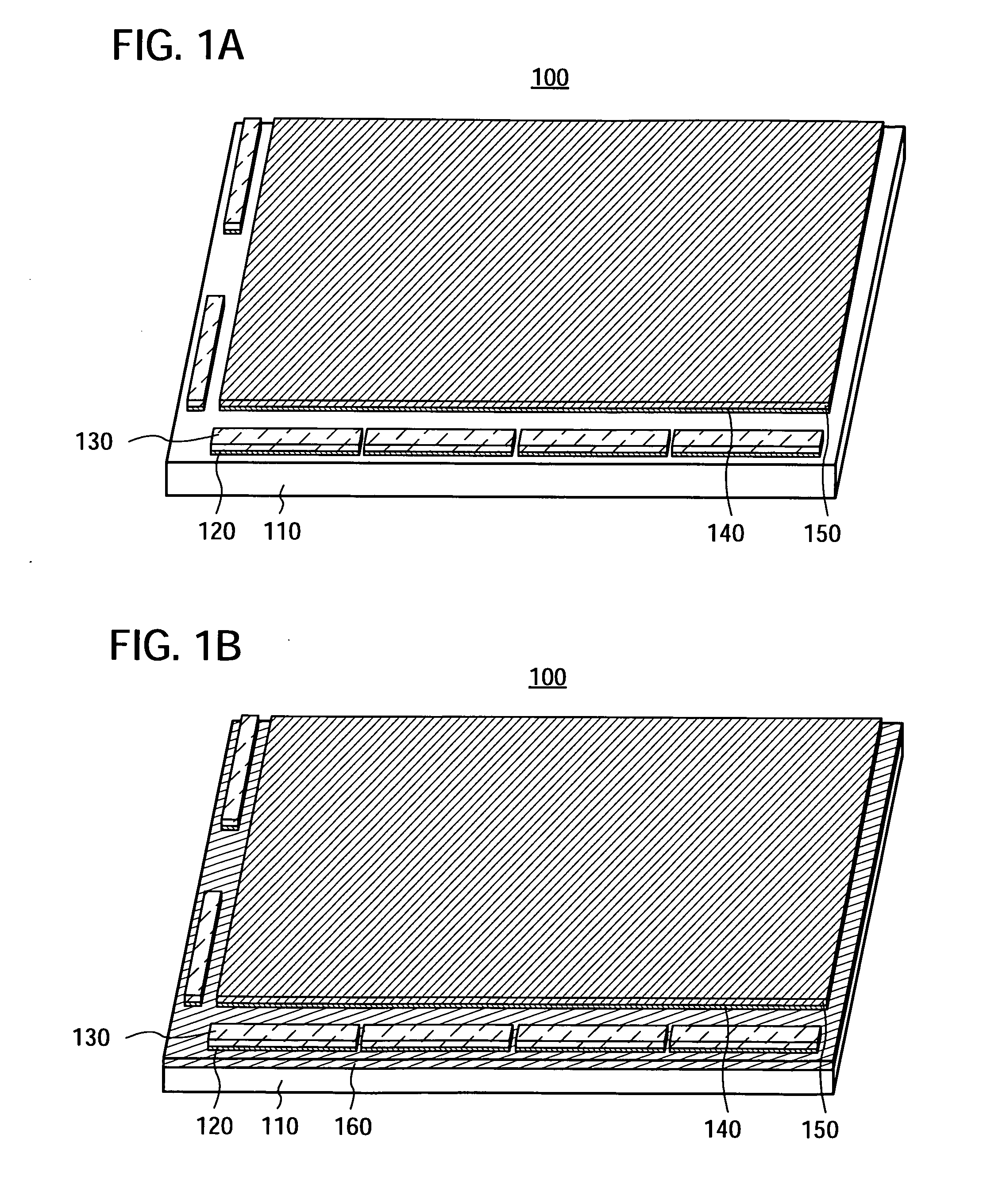
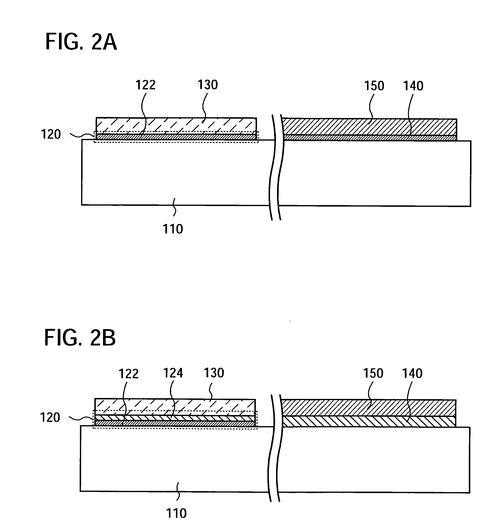
[0046]FIGS. 1A and 1B are each a perspective view of a semiconductor substrate used in the present invention. In addition, FIGS. 2A and 2B and FIGS. 3A and 3B are each a cross-sectional view of a semiconductor substrate used in the present invention.

[0047]In FIGS. 1A, 2A, and 2B, a semiconductor substrate 100 has a structure in which, on one surface of a base substrate 110, a plurality of stacks in each of which insulating layers 120 and single-crystal semiconductor layers 130 are sequentially stac...

embodiment mode 2

[0095]This embodiment mode will describe below a method for manufacturing a liquid crystal display device using a semiconductor substrate which is manufactured in Embodiment Mode 1 with reference to FIGS. 8A to 8C, FIGS. 9A to 9D, FIGS. 10A to 10C, and FIGS. 11A to 11C.

[0096]FIG. 8A is a top view of a liquid crystal display device. FIG. 8B is a cross-sectional view taken along line OP of FIG. 8A. FIG. 8C is a perspective view of a liquid crystal display device.

[0097]A liquid crystal display device according to this embodiment mode includes a display portion 820, a first driver circuit portion 830, and a second driver circuit portion 850 over a first substrate 800. The display portion 820, the first driver circuit portion 830, and the second driver circuit portion 850 are sealed with a sealant 880 between the first substrate 800 and a second substrate 890. Further, a terminal region 870 where an external input terminal which transmits signals from the outside to the first driver circ...

embodiment mode 3

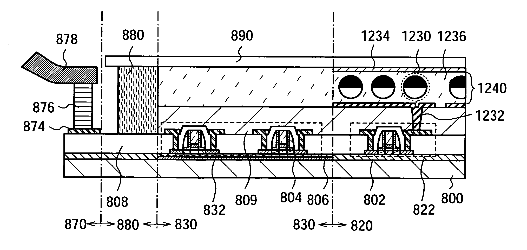
[0152]Embodiment Mode 2 shows an example in which a display device which uses a liquid crystal display device is manufactured; however, this embodiment mode will describe another display device with reference to FIGS. 12A and 12B.

[0153]FIG. 12A illustrates an example of a display device using a light-emitting element (also referred to as a light-emitting device or an EL display device). FIG. 12B illustrates an example of a display device using an electrophoretic element (also referred to as electronic paper or an electrophoretic display device). Note that detailed description thereof is omitted because structures other than those of display elements are similar to those shown in Embodiment Mode 2.

[0154]FIG. 12A illustrates a display device using a light-emitting element 1210 instead of a liquid crystal element. Here, an example is shown in which an organic compound layer 1214 is provided between a pixel electrode (cathode) 1212 and a counter electrode (anode) 1216. The organic compo...


PUM


Abstract

A method for manufacturing a semiconductor device provided with a circuit capable of high speed operation while the manufacturing cost is reduced. A method for manufacturing a semiconductor device which includes forming an ion-doped layer at a predetermined depth from a surface of a single-crystal semiconductor substrate and forming a first insulating layer over the single-crystal semiconductor substrate; forming a second insulating layer over part of an insulating substrate and forming a non-single-crystal semiconductor layer over the second insulating layer; bonding the single-crystal semiconductor substrate to a region of the insulating substrate where the second insulating layer is not formed, with the first insulating layer interposed therebetween; and forming a single-crystal semiconductor layer over the insulating substrate by separating the single-crystal semiconductor substrate at the ion-doped layer which acts as a separation surface so that the ion-doped layer is separated from the insulating substrate.

Description

BACKGROUND OF THE INVENTION[0001]1. Field of the Invention[0002]The present invention relates to methods for manufacturing a semiconductor device, methods for manufacturing a display device, semiconductor devices, display devices, and electronic devices.[0003]2. Description of the Related Art[0004]In recent years, flat panel displays such as liquid crystal display devices and electroluminescence (EL) display devices have attracted attention.[0005]Driving methods of the flat panel displays include a passive matrix method and an active matrix method. An active matrix method has advantages over a passive matrix method in low power consumption, high definition, a large-sized substrate, and the like.[0006]Here, a structural example of an active matrix display device is briefly described with reference to FIGS. 14A and 14B. FIG. 14A illustrates an example of a structure in which a driver circuit is provided using a tape automated bonding (TAB) method.[0007]In FIG. 14A, a pixel portion 140...

Claims


Application Information

Patent Timeline
IPC IPC(8): H01L33/00H01L21/00G02F1/1345G02F1/1368H01L21/02H01L21/20H01L21/265H01L21/336H01L27/12H01L29/786
CPCH01L21/02683H01L21/02686H01L29/66772H01L27/1214H01L27/1266H01L21/76254H01L27/1229
Inventor HONDA, TATSUYA
Owner SEMICON ENERGY LAB CO LTD
Why Eureka
Try Eureka