
Trap read only non-volatile memory (TROM)

a non-volatile memory and read-only technology, applied in the direction of logic circuits, instruments, pulse techniques, etc., can solve the problems of poor data retention and slow erase speed, poor data retention, and roadblocks in slow erase speed, etc., to achieve the effect of improving data retention, easy scaling with small and small design rules, and suitable for very high-density memory

Active Publication Date: 2005-08-04
MACRONIX INT CO LTD
View PDF24 Cites 27 Cited by
  • Summary
  • Abstract
  • Description
  • Claims
  • Application Information

AI Technical Summary

Benefits of technology

[0007] A Trap Read Only Memory (TROM) architecture is provided. Embodiments of the TROM employ a NAND-type array structure, making it easy to scale with smaller and smaller design rules and therefore suitable for very high-density memory. Embodiments of the TROM employ an E-field assisted (Fowler-Nordheim FN) tunneling program algorithm, and require only low voltage or ground biasing on the source / drain channel terminals of the cell while programming. A thicker tunneling oxide on the TROM cell gives better data retention than conventional SONOS NAND-type memory cell structures and the floating gate free cell structures. Embodiments of the TROM are configured as read only memory devices, such that the memory cells are programmed one time only, and there is no erase cycle. With no erase cycles, damage to the tunneling dielectric is avoided, and charge retention and read endurance performance is very good. As a result better data retention and better cell scalability are achieved, compared to conventional NAND flash memory or SONOS NAND-type memory.
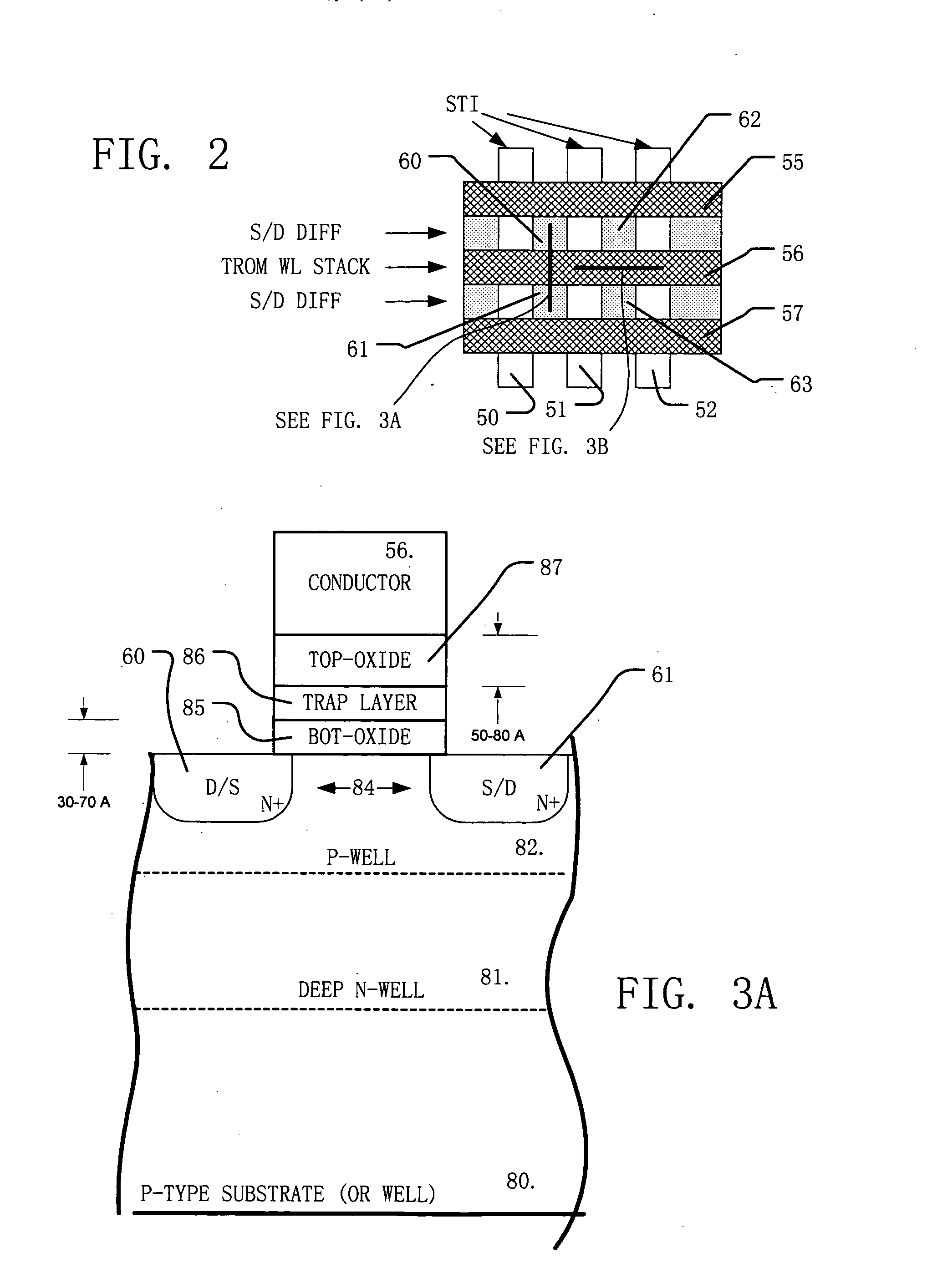
[0009] The integrated circuit according to this embodiment of the invention includes circuitry to program memory cells in the array by E-field assisted tunneling from the channel region through the tunneling dielectric by applying a positive voltage to the gate terminal and a low voltage or ground to semiconductor bulk region in which the channel is formed, and to the first and second channel terminals. The tunneling dielectric has a barrier thickness relative to the semiconductor substrate that is sufficient to prevent direct tunneling. Thus, for a silicon dioxide based tunneling dielectric, the tunneling dielectric has a thickness greater than about 30 Angstroms. For other dielectric materials, the thickness can be characterized based on silicon dioxide equivalent thickness of about 30 Angstroms as well. In embodiments of the invention, the tunneling dielectric has a thickness that is less than about 70 Angstroms, and more preferably less than about 60 Angstroms. With a tunneling dielectric having a thickness between about 30 and about 70 Angstroms, E-field assisted tunneling can be efficiently accomplished on integrated circuit with reasonable voltages, without requiring other charge carrier energy boosting techniques, such as applied for hot electron programming.
[0010] When programming according to embodiments of the invention, a positive bias is applied on the word line establishing a big electric field between the word line and the channel, for example 18V across 5 nm, and assisting the electron tunneling into the trapping layer. The electric field causes the energy band to bend across the tunnel dielectric, so that its effective thickness is reduced enough to allow tunneling. Unlike SONOS-type NAND arrays, the tunnel dielectric has a thickness that is sufficient to prevent direct tunneling (greater than 30 Angstroms silicon dioxide equivalent thickness), improving data retention. Unlike the NROM array, the tunnel dielectric in the TROM is less than 70 Angstroms silicon dioxide equivalent thickness, and in some embodiments less than 60 Angstroms silicon dioxide equivalent thickness, allowing E-field assisted tunneling in practical program times and voltages, and improving scalability while retaining excellent data retention.

Problems solved by technology

However, as design rules have scaled down toward 70 nanometers, and below, floating gate type NAND flash memory becomes impractical due to poor endurance, and parasitic capacitance between adjacent floating gates which deteriorates the cell threshold voltage distribution.
However, poor data retention and slow erase speed remain roadblocks for the application of the SONOS cell for high density NAND flash memory.

Method used


Image

  • Trap read only non-volatile memory (TROM)
  • Trap read only non-volatile memory (TROM)
  • Trap read only non-volatile memory (TROM)

Examples


Embodiment Construction

[0028] A detailed description of embodiments of the present invention is provided with reference to FIGS. 1-10.

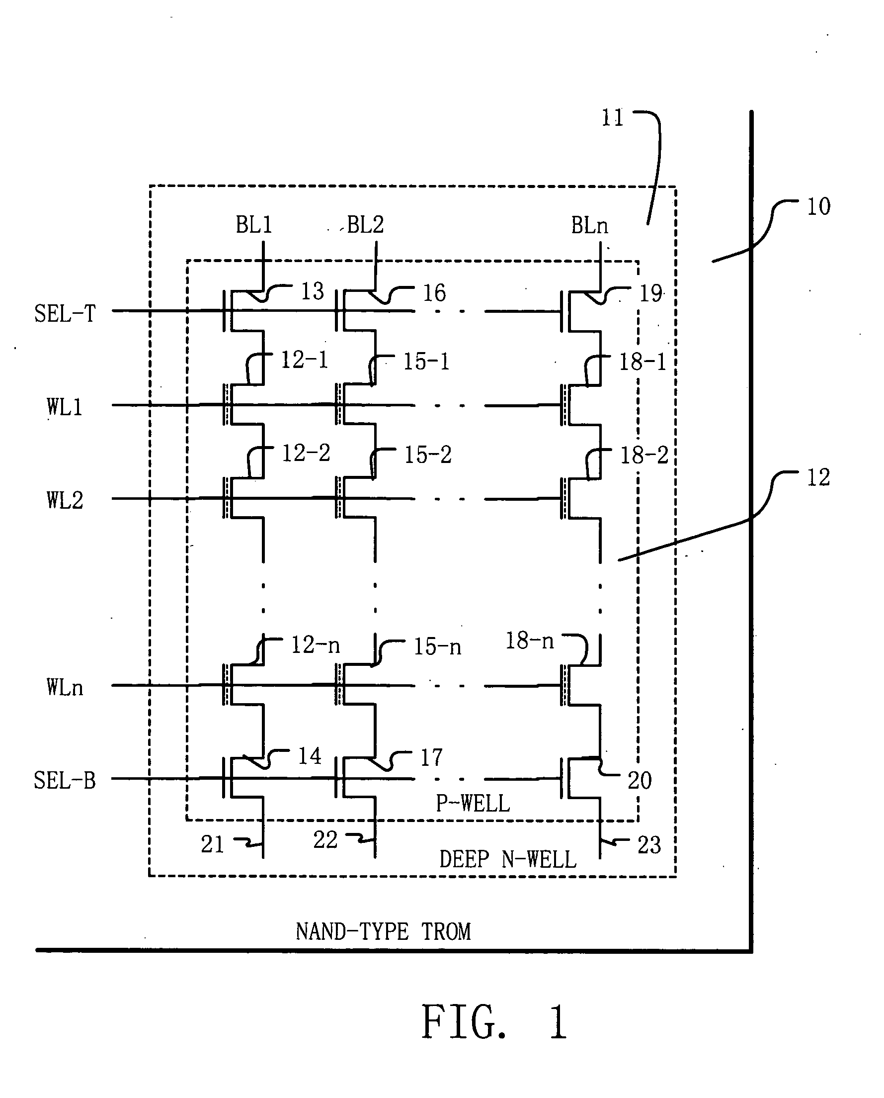
[0029]FIG. 1 illustrates a basic NAND array architecture implemented with TROM cells according to the present invention. As shown in FIG. 1, the TROM NAND array comprises a plurality of memory cells configured in columns and rows. The columns comprise sets of memory cells that are arranged in series, and which have select transistors on one or both ends of the set for coupling the set of memory cells to bit lines. Thus, as shown in FIG. 1, a first bit line BL1 is coupled via a top select transistor 13 to a set of memory cells 12-1, 12-2, . . . 12-n connected in series. At the opposite end of the set of memory cells, a select transistor 14 is provided. The select transistors 13, 14 are responsive to decoded block select signals SEL-T at the top of the set, and SEL-B at the bottom of the set. The select transistor 13 typically connects directly to the bit line BL1, while the...


PUM


Abstract

A Trap Read Only Memory (TROM) architecture employs a NAND-type array structure configured as a read-only memory that is programmed only one time. The memory cells in the array comprise a gate terminal, a first channel terminal (source / drain), a second channel terminal (drain / source) and a channel region between the first and second channel terminals. A charge trapping structure, such as a layer of silicon nitride, is formed over the channel region. A tunneling dielectric is placed between the channel region and the charge trapping structure, and a blocking dielectric is placed between the charge trapping structure and the gate terminal. An E-field assisted (Fowler-Nordheim FN) tunneling program algorithm is applied.

Description

BACKGROUND OF THE INVENTION [0001] 1. Field of the Invention [0002] The present invention relates to electrically programmable, non-volatile, read-only memory and integrated circuits including such memory, and more particularly to a memory cell structure and method of operation based upon charge trapping structures adapted for E-field assisted tunneling. [0003] 2. Description of Related Art [0004] Electrically programmable non-volatile memory technologies are being adapted to many applications. The various technologies vary in the number of times that the memory cells can be programmed, the voltages required to achieve programming, and the number of bits of data stored in each memory cell. Also, an important consideration in determining whether to apply a particular memory technology is the manufacturing steps required to form the memory cells and supporting circuitry. [0005] Memory technologies also vary according to the array architecture. One popular architecture is known as the ...

Claims


Application Information

Patent Timeline
IPC IPC(8): G11C16/04H01L29/51H01L29/792H10B69/00
CPCG11C16/0466G11C16/0483H01L29/792H01L29/513H01L27/115H10B69/00
Inventor LUNG, HSIANG LAN
Owner MACRONIX INT CO LTD
Learn More