High frequency power amplifier circuit
a power amplifier and circuit technology, applied in the field of high frequency power amplifier circuits, can solve the problems of difficult to difficult to miniaturize the module, and large power loss, so as to improve the detection sensitivity of output power, prevent excessive output power from becoming excessive, and reduce the size of the modul
- Summary
- Abstract
- Description
- Claims
- Application Information
AI Technical Summary
Benefits of technology
Problems solved by technology
Method used
Image
Examples
first embodiment
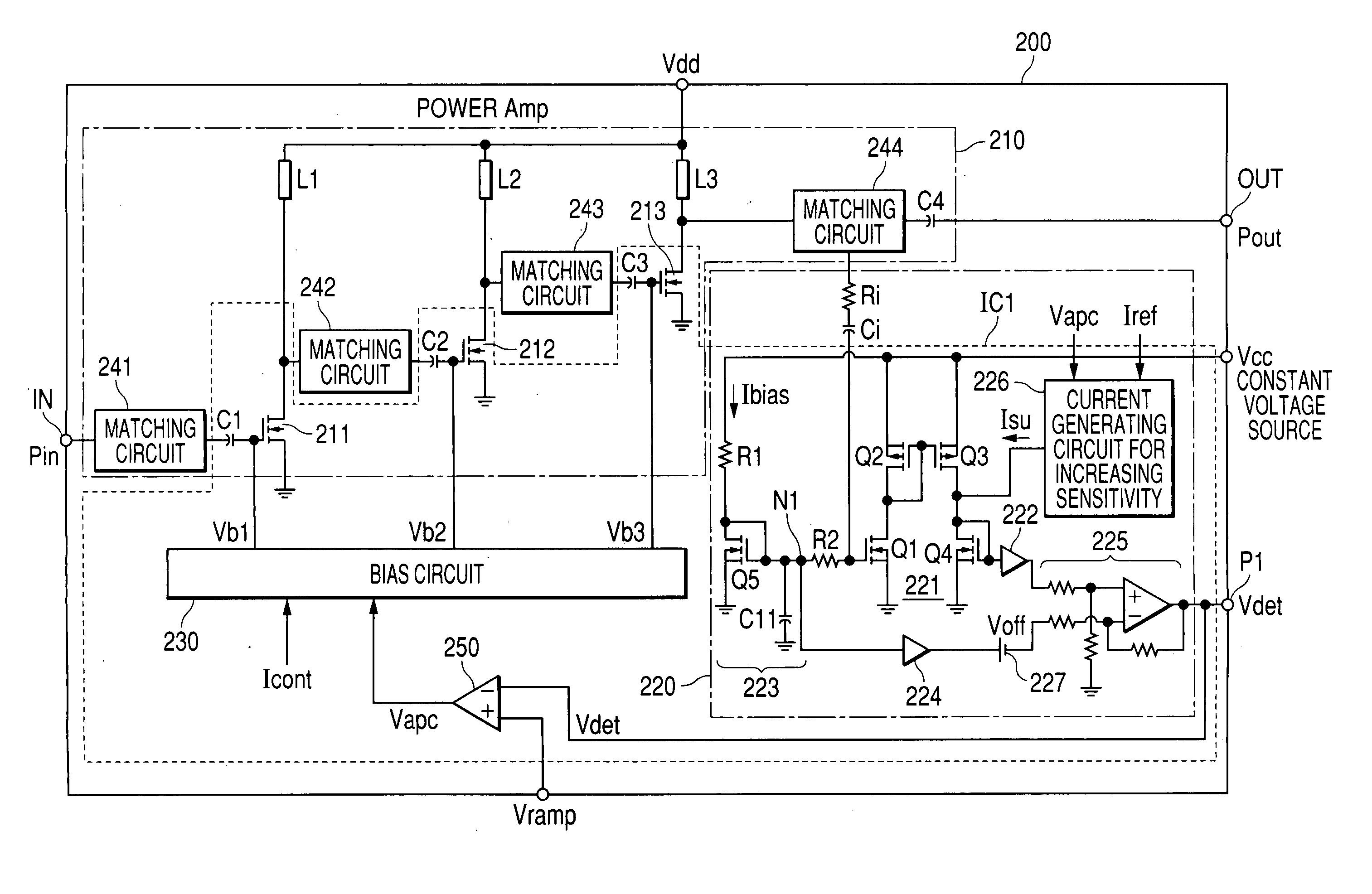
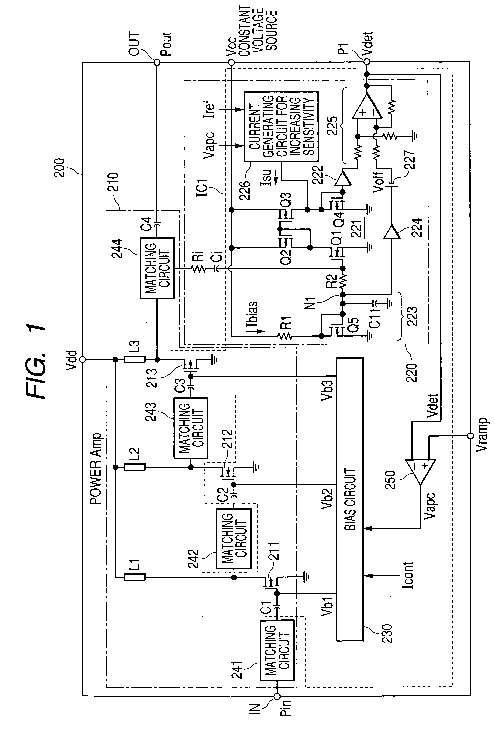
[0031]FIG. 1 shows an embodiment of a high frequency power amplifier (hereinbelow, called power module) to which an output power detection circuit of the invention is applied. In the specification, a structure constructed so as to be handled as a single electronic part by mounting a plurality of semiconductor chips and discrete parts on an insulating substrate such as a ceramic board on / in which print wiring is conducted and connecting the parts via the print wiring and bonding wires so that each part plays a predetermined role is called a module.
[0032] A power module 200 of the embodiment has a high frequency power amplifier 210 including a power amplification FET for amplifying an input high frequency signal Pin, an output power detection circuit 220 for detecting output power of the high frequency power amplifier 210, a bias circuit 230 for applying a bias voltage to the power amplification FET in each of stages of the high frequency power amplifier 210, thereby controlling idle...
second embodiment
[0058]FIG. 7 shows a second embodiment of a power module to which the output power detection circuit of the invention is applied. In FIG. 7, the same reference numeral is designated to a circuit or device which is the same as that shown in FIGS. 1 and 2 and its description will not be repeated.
[0059] In the second embodiment, an operation point is given to the gate terminal of the transistor 213 for amplification in the final stage by a voltage obtained by dividing the output control voltage Vapc output from the error amplifier 250 by the resistors R31 and R32. Although not shown, an optimum operation point is given to each of the gate terminals of the transistors 211 and 212 for amplification in the first and second stages by a voltage obtained by dividing the output control voltage Vapc by the resistors at a different resistance ratio. In the second embodiment, the bias circuit 230 for applying the gate bias voltage of the transistors 211 to 213 for amplification is constructed b...
example of application
[0077]FIG. 12 shows a schematic configuration of a system capable of performing two radio communications in two communication systems of GSM and DCS as an example of a radio communication system which is effective when the power module of the embodiment is applied.
[0078] In FIG. 12, ANT denotes an antenna for transmitting / receiving signal electric waves, and 100 denotes an electronic device (hereinbelow, called an RF device) obtained by mounting, into a single package, a high frequency signal processing circuit (baseband circuit) 110 having a modulation / demodulation circuit capable of performing GMSK modulation and demodulation in the GSM and DCS systems and a circuit for generating I and Q signals on the basis of transmission data (baseband signal) and processing I and Q signals extracted from a reception signal, a semiconductor integrated circuit (baseband IC) for processing high frequency signals obtained by forming low noise amplifiers LNA1 and LNA2 for amplifying reception sig...
PUM
 Abstract
Description
Claims
Application Information
 - R&D
- Intellectual Property
- Life Sciences
- Materials
- Tech Scout
- Unparalleled Data Quality
- Higher Quality Content
- 60% Fewer Hallucinations
Browse by: Latest US Patents, China's latest patents, Technical Efficacy Thesaurus, Application Domain, Technology Topic, Popular Technical Reports.
© 2025 PatSnap. All rights reserved.Legal|Privacy policy|Modern Slavery Act Transparency Statement|Sitemap|About US| Contact US: help@patsnap.com


