Method of manufacturing ESD protection component

Inactive Publication Date: 2005-06-30
PANASONIC CORP
View PDF14 Cites 9 Cited by
  • Summary
  • Abstract
  • Description
  • Claims
  • Application Information

AI Technical Summary

Benefits of technology

[0010] The method of manufacturing an ESD protection component according to the present invention includes at least a step of producing slurry by mixing varistor particles, a resin binder, a plasticizer, and a solvent; a step of producing a varistor green sheet by coating a film with the slurry and then drying it; a step of forming a conductor layer; a step of forming an adhesive layer including a resin as its principal component, on at least one side of a ceramic substrate; a step of sticking the varistor green sheet on the adhesive layer; and a step of baking at a temperature at which the varistor particles substantively sinter. The invention provides a method of manufacturing high-performance, small-variation ESD protection components.BRIEF DESCRIPTION OF THE DRAWINGS

Problems solved by technology

Consequently, the number of failures is increasing where static pulses occurring when a human body touches a terminal of an electronic device destroy an electronic part inside the electronic device.
Therefore, a large number of cracks and holes occur inside a varistor film formed with conventional screen-printing, and areas without insulating films at grain boundaries of semiconductor particles like zinc oxide will increase as well.
Thus, a high-performance varistor characteristic cannot be achieved with screen printing.
In addition, the varistor characteristic was not uniform and reliability was low.

Method used


Image

  • Method of manufacturing ESD protection component
  • Method of manufacturing ESD protection component
  • Method of manufacturing ESD protection component

Examples


first embodiment

[0030] A detailed description is made for a method of manufacturing an ESD protection component according to the first embodiment of the present invention, using an example.

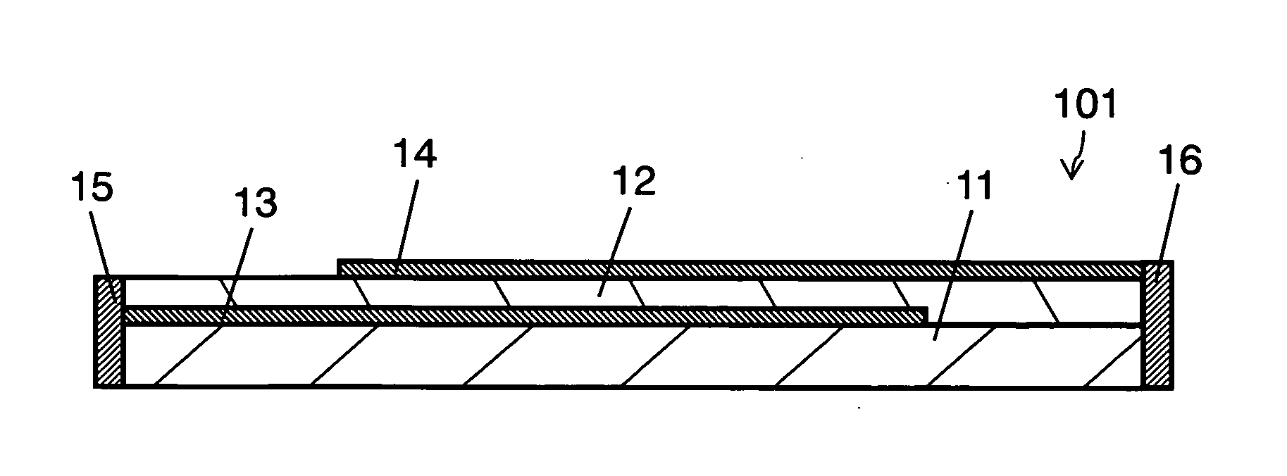
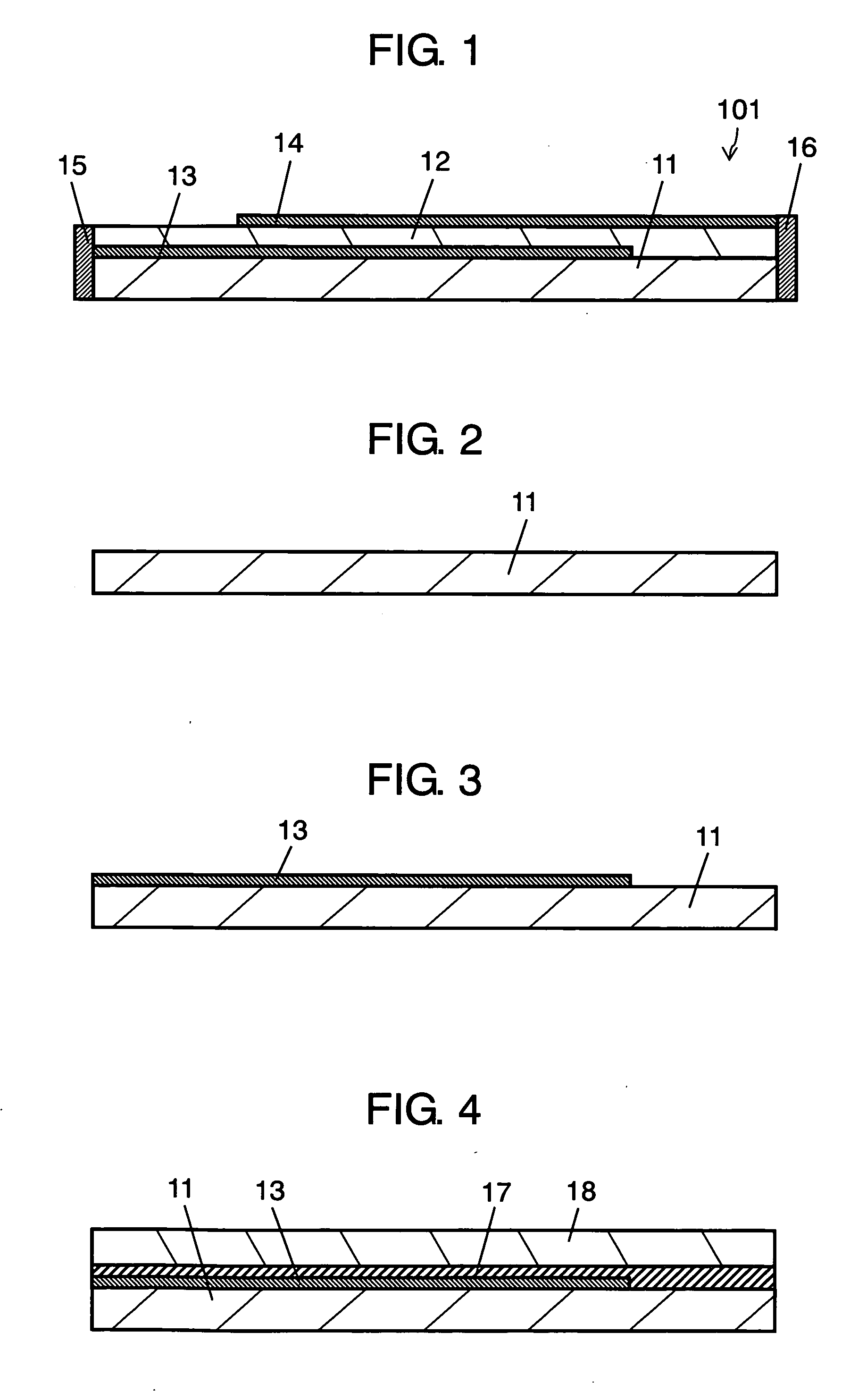
[0031]FIG. 1 is a sectional view illustrating ESD protection component 101 in example 1, according to the first embodiment of the present invention.

[0032] ESD protection component 101 includes ceramic substrate 11, varistor layer 12, conductor layers 13 and 14, and terminal electrodes 15 and 16. In other words, conductor layer 13 is formed with a conductive material such as silver, on ceramic substrate 11 such as 96% alumina, a layer made of a varistor material is formed thereon, and baked, to produce varistor layer 12. Further, conductor layer 14 is provided on this varistor layer 12 to form a varistor element in which varistor layer 12 is sandwiched by conductor layers 13 and 14. Finally, terminal electrodes 15 and 16 that connect to conductor layers 13 and 14, respectively, are provided at both ends of subst...

second embodiment

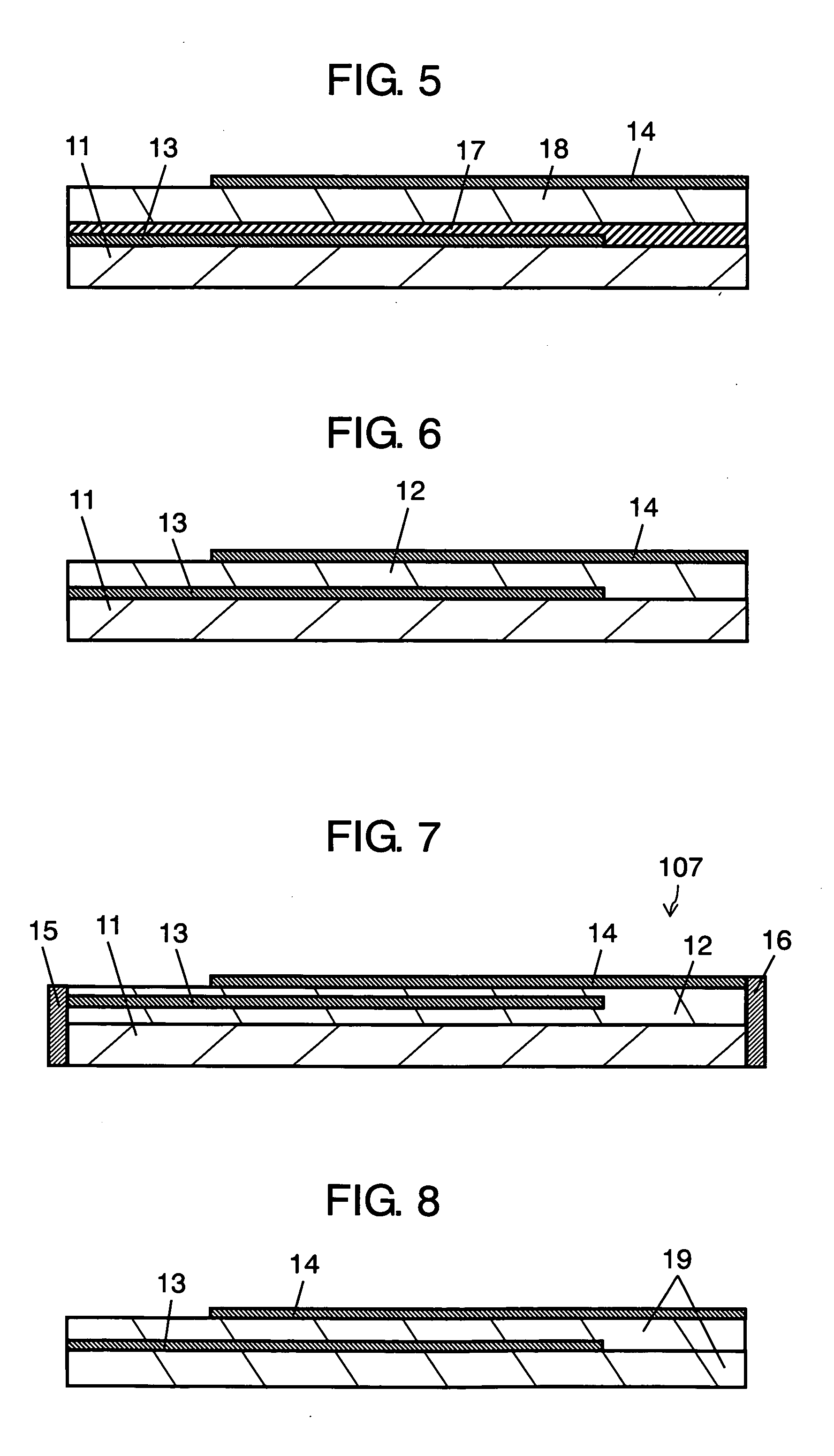
[0057] In the second embodiment of the present invention, a description is made for the component of adhesive to be used for adhesive layer 17. In the first embodiment, adhesive layer 17 is formed using a solution of polyvinyl butyral and dibutyl phthalate mixed at a weight ratio of 1:10. Varistor particles, and inorganic materials, namely constituent materials for varistor particles, such as zinc oxide, bismuth oxide, cobalt oxide, manganese oxide, or antimony oxide, are dispersed in the solution.

[0058] Table 2 compares the characteristics of an ESD protection component, when changing the kind of an inorganic material dispersed in adhesive layer 17, and its added amount (added amount per 100 g of adhesive). Ten pieces of ESD protection components 107 are produced per each condition using substrates with 15 cm×15 cm. The probability that peeling occurs after baking and the average value of the varistor characteristics a are measured as evaluation items.

[0059] As shown in table 2, ...

third embodiment

[0062] The third embodiment of the present invention describes a relation of the porosity of varistor green sheet 19 shown in FIG. 8 with adhesiveness on alumina substrate 11 and with the varistor characteristic. The porosity of varistor green sheet 19 used in the third embodiment of the present invention is obtained from equation 1 described below.

[0063] In the third embodiment, the pressing pressure and temperature in the transferring or laminating step are changed to control the porosity of varistor green sheet 19. (Porocity)=1-Apparent_density⁢_of⁢_green⁢_seatWeight_of⁢_varister⁢_partcles+Weight_of⁢_binder+Weight_of⁢_plasticize⁢ ⁢rWeight_of⁢_varister⁢_partclesDensity_of⁢_varister+Weight_of⁢_binderDensity_of⁢_binder+Weight_of⁢_plasticize⁢ ⁢rDensity_of⁢_plasticize⁢ ⁢r(Formula⁢ ⁢_⁢1)

[0064] Ten pieces of ESD protection components 107 shown in FIG. 7 are produced using a layered product of varistor green sheet 19, and the relation is evaluated between the probability that peeling o...


PUM

PropertyMeasurementUnit
Diameteraaaaaaaaaa
Diameteraaaaaaaaaa
Porosityaaaaaaaaaa

Abstract

The present invention relates to a method of manufacturing an ESD protection component, where the method includes at least a step of producing slurry including varistor particles and a resin binder; a step of producing a varistor green sheet from this slurry; a step of forming a conductor layer; a step of forming an adhesive layer on a ceramic substrate; a step of sticking a varistor green sheet on an adhesive layer; and a step of baking, providing a high-performance and uniform ESD protection component.

Description

BACKGROUND OF THE INVENTION [0001] 1. Field of the Invention [0002] The present invention relates to an ESD protection component that protects an electronic device against static electricity. [0003] 2. Background Art [0004] The withstand voltage of an electronic part used for an electronic device is becoming low with a rapid progress in downsizing and higher performance of an electronic device such as a mobile phone. Consequently, the number of failures is increasing where static pulses occurring when a human body touches a terminal of an electronic device destroy an electronic part inside the electronic device. [0005] Conventionally, the following method has been well known for protecting from such static pulses. That is to say, provide a laminated chip varistor or Zener diode between a line to which static electricity is input and the ground, to bypass static electricity for suppressing a voltage applied to an electronic part inside an electronic device. [0006] In addition, a grow...

Claims


Application Information

Patent Timeline
IPC IPC(8): H01C7/10H01C17/00H01C7/112H01C17/06H01C17/065
CPCH01C7/1006H01C17/06586H01C17/06546H01C7/112H01C7/10H01C17/06
Inventor KATSUMURA, HIDENORIINOUE, TATSUYAKAGATA, HIROSHI
Owner PANASONIC CORP
Why Eureka
Try Eureka