
Photosensitive lacquer for providing a coating on a semiconductor substrate or a mask

a technology of photosensitive lacquer and semiconductor substrate, which is applied in the direction of photosensitive materials, auxiliaries/base layers of photosensitive materials, instruments, etc., can solve the problems of insufficient sidewall passivation, limited wavelength range of resists used in photolithographic structuring, and rough edges leading to a particular extent of sidewall roughness, etc., to achieve the effect of improving quality

Inactive Publication Date: 2005-06-16
POLARIS INNOVATIONS
View PDF18 Cites 16 Cited by
  • Summary
  • Abstract
  • Description
  • Claims
  • Application Information

AI Technical Summary

Benefits of technology

[0010] It is therefore the object of the present invention to provide a resist system that reduces the above-mentioned problems and permits an improvement in the quality on transfer of the structure of resist structures to underlying coats.
[0016] According to two advantageous developments, at least two base polymers are present as block copolymers, or they are present together in a blend without chemical bonds being established. It was found that, by means of the resist according to the invention, the advantages applicable in each case for their wavelength range can also be utilized in a blend or block copolymer formation of the at least two polymer substances for effecting structure transfer with high resolution if also only one of the wavelengths, in particular 193 nm, is used for the incident light. The respective volume fractions of the base polymers and the total coat thickness of the resist are to be chosen so that, in spite of the absorption property of the one base polymer at the given light wavelength, exposure down to the bottom surface of the resist is ensured.
[0017] If, for example, a second base polymer having aromatic parent structures and provided with a lower mole fraction in comparison with the first base polymer having cycloaliphatic parent structures is used at an exposure wavelength of 193 nm, this gives rise to an advantage that an interaction of the resist with the substrate is reduced. Consequently, resist residues after an exposure and development process in the exposed structures are considerably reduced. This is due to the polymer components of the second base polymer containing the aromatic parent structures.
[0018] The additional fractions of the second polymer also ensure that the roughness of the resist sidewalls after an etching process is reduced owing to the aromatic moiety. The reason for this is an improved fluorine sidewall passivation in the exposed structures, which leads firstly to increased stability of remaining walls as well as to dimensionally stable structure transfer. Moreover, the so-called etch bias, a reserve for the etching which has to be used for compensating the effect described, is thus likewise advantageously reduced. A further advantage is the increased etch resistance which is provided by the aromatic moiety, for reducing the resist thickness and consequently for the stability of the resist mask.
[0019] On the other hand, the total absorption or the depth of penetration of the incident light is influenced only to an insignificant extent by the absorption properties, owing to the small mole fraction of the second base polymer comprising the aromatic parent structures. Only with slight additional process complexity, this could be compensated by a reduced resist thickness, and increased light intensity or a longer exposure time.

Problems solved by technology

In general, however, the resists used in the photolithographic structuring are transparent only over a limited wavelength range.
However, the resists still give rise to considerable problems in the transfer of the structure to the substrate.
Thus, for example in the case of the exposed and developed structures, roughened edges leading to insufficient passivation of the sidewalls occur to a particular extent.
Owing to a reduced stability of the resist walls remaining after the development, they may collapse, for example, also in a subsequent measurement of the structure width in a scanning electron microscope.
A further disadvantage arises by virtue of the fact that conventional resists transparent at a wavelength of 193 nm interact chemically with the antireflection coats underneath them, so that resist residues within the tracks between the resist walls may occur.
However, this leads to a considerably increased process complexity.

Method used


Image

  • Photosensitive lacquer for providing a coating on a semiconductor substrate or a mask
  • Photosensitive lacquer for providing a coating on a semiconductor substrate or a mask

Examples


Embodiment Construction

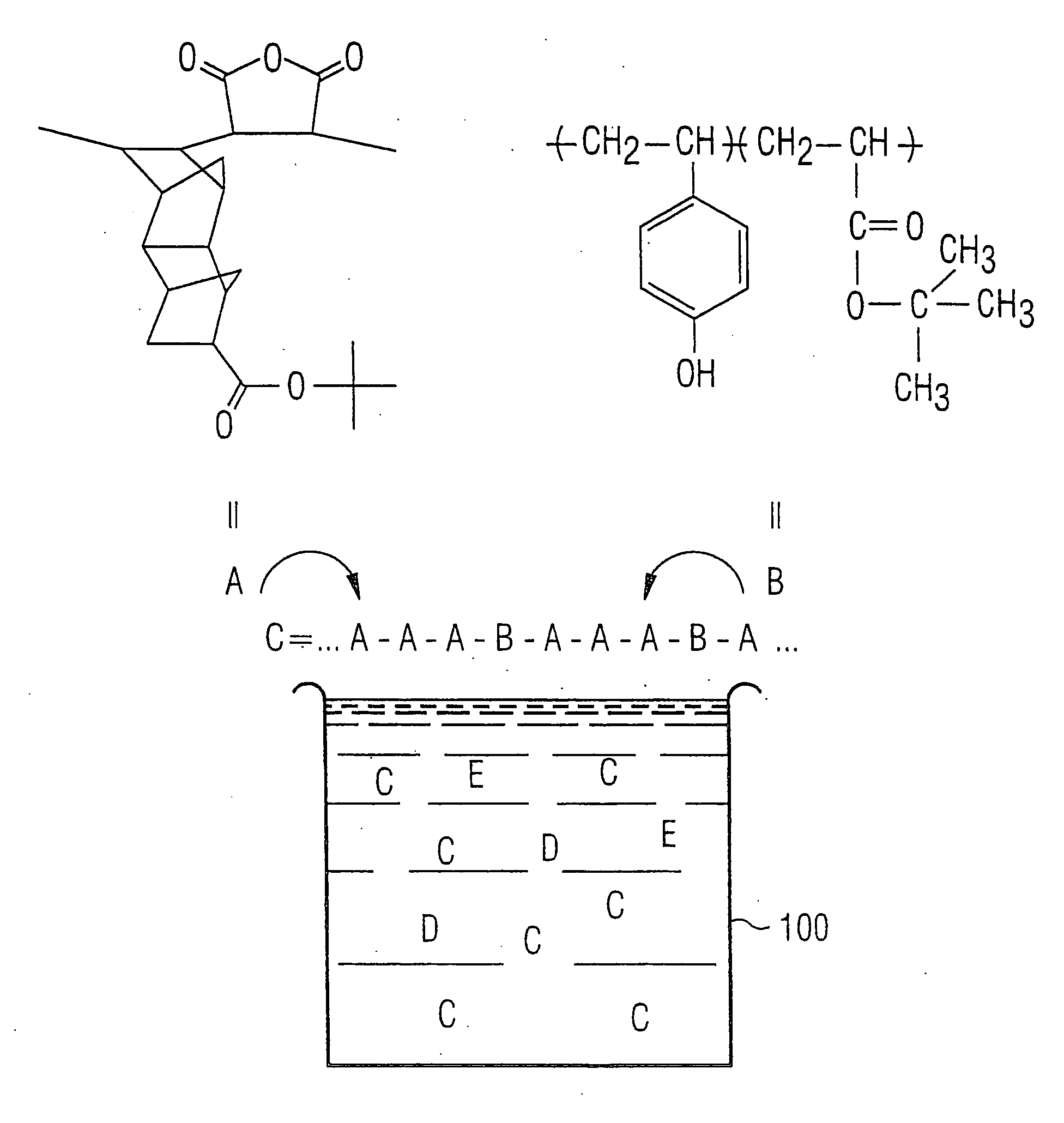
[0030] The FIGURE shows a photosensitive resist 100 with solvents E, acid generators D and with first base polymers which are synthesized as block copolymers C and comprise cycloaliphatic parent structures A, and second base polymers which comprise aromatic parent structures B. The fraction of the second base polymers containing aromatic parent structures B, based on all base polymers A, B, is 5 mol %. In this embodiment, the second base polymer having aromatic parent structures B comprises poly(4-hydroxystyrene), which is blocked by acid-sensitive tert-butoxycarbonyl groups.

[0031] The first base polymer having the cycloaliphatic parent structures A comprises an acid-sensitive blocking group, which in this case is a polymethacrylate. It also comprises an alkali-soluble unit of cycloolefinmaleic anhydride.

[0032] The resist is prepared with a polymer synthesis using the stated mole fractions of the base polymers. This resist is applied to a wafer in a coat thickness of 100-150 nm, p...


PUM

PropertyMeasurementUnit
thicknessaaaaaaaaaa
thicknessaaaaaaaaaa
wavelengthaaaaaaaaaa

Abstract

A photosensitive resist (100) for coating on a semiconductor substrate or a mask comprises a photo acid generator (D), a solvent (E) and at least two different base polymers, of which a first base polymer comprises cycloaliphatic parent structures (A) which substantially absorb incident light at 248 nm and are substantially transparent to incident light at 193 nm, and a second base polymer comprises aromatic parent structures (B) which substantially absorb incident light at 193 nm and are substantially transparent to incident light at 248 nm. If such a resist (100) is applied in a coat thickness of from 50 to 400 nm to a substrate and the proportion of the second base polymer having the aromatic parent structure is between 1 and 25 mol %, a relatively high structure contrast, better stability to etching and a reduction of defects are advantageously achieved in an exposure at a wavelength of 193 nm. Exposure over the entire depth range of the resist (100) is ensured thereby.

Description

[0001] This application is a continuation of co-pending International Application No. PCT / DE03 / 01781, filed May 30, 2003, which designated the United States and was not published in English, and which is based on German Application No. 102 24 217.8 filed May 31, 2002, both of which applications are incorporated herein by reference.TECHNICAL FIELD [0002] The present invention relates to photosensitive resist for coating on a semiconductor substrate or a mask. BACKGROUND [0003] For the production of integrated circuits in the semiconductor industry, semiconductor substrates or masks, as precursors for the exposure of the semiconductor substrates to light, are coated with photosensitive resists, which are then exposed to light in a photolithographic step with a structure representing a component of the circuit. Depending on the formation of the resist as a positive or negative resist, the exposed or unexposed structures are used, after a development step, as an etch or implantation mas...

Claims


Application Information

Patent Timeline
Patent Type & Authority Applications(United States)
IPC IPC(8): G03C1/492G03C1/494G03C1/76G03F7/039H01L21/31H01L21/469
CPCG03F7/0395G03F7/0392
Inventor ROGALLI, MICHAELVOLKEL, LARS
Owner POLARIS INNOVATIONS
Learn More