Light receiving element and light receiving device incorporating circuit and optical disk drive
- Summary
- Abstract
- Description
- Claims
- Application Information
AI Technical Summary
Benefits of technology
Problems solved by technology
Method used
Image

Examples
first embodiment
THE FIRST EMBODIMENT
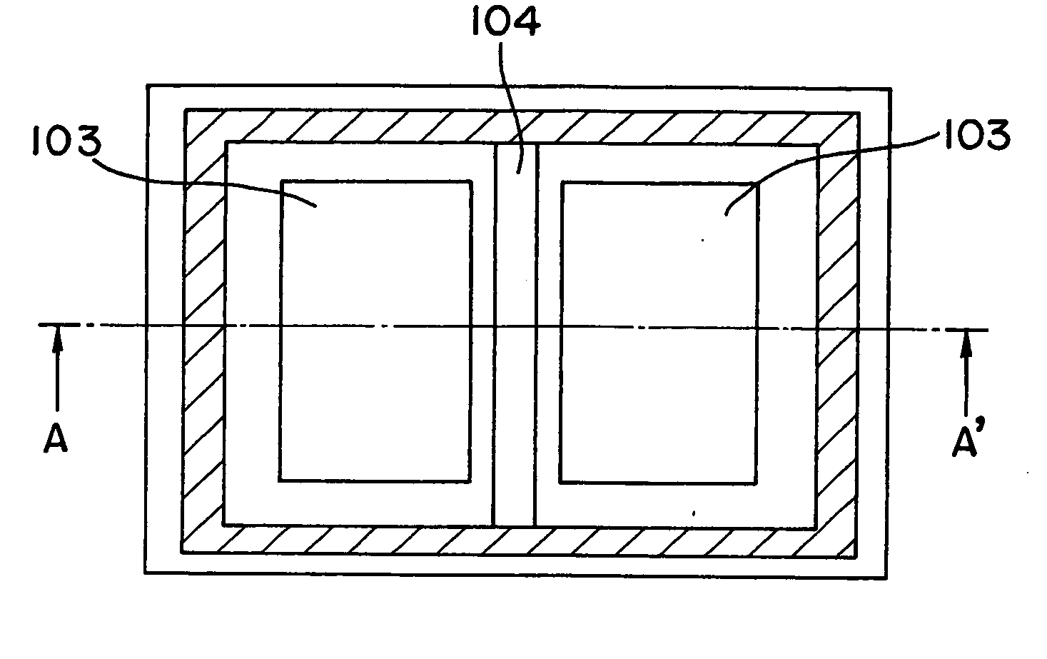
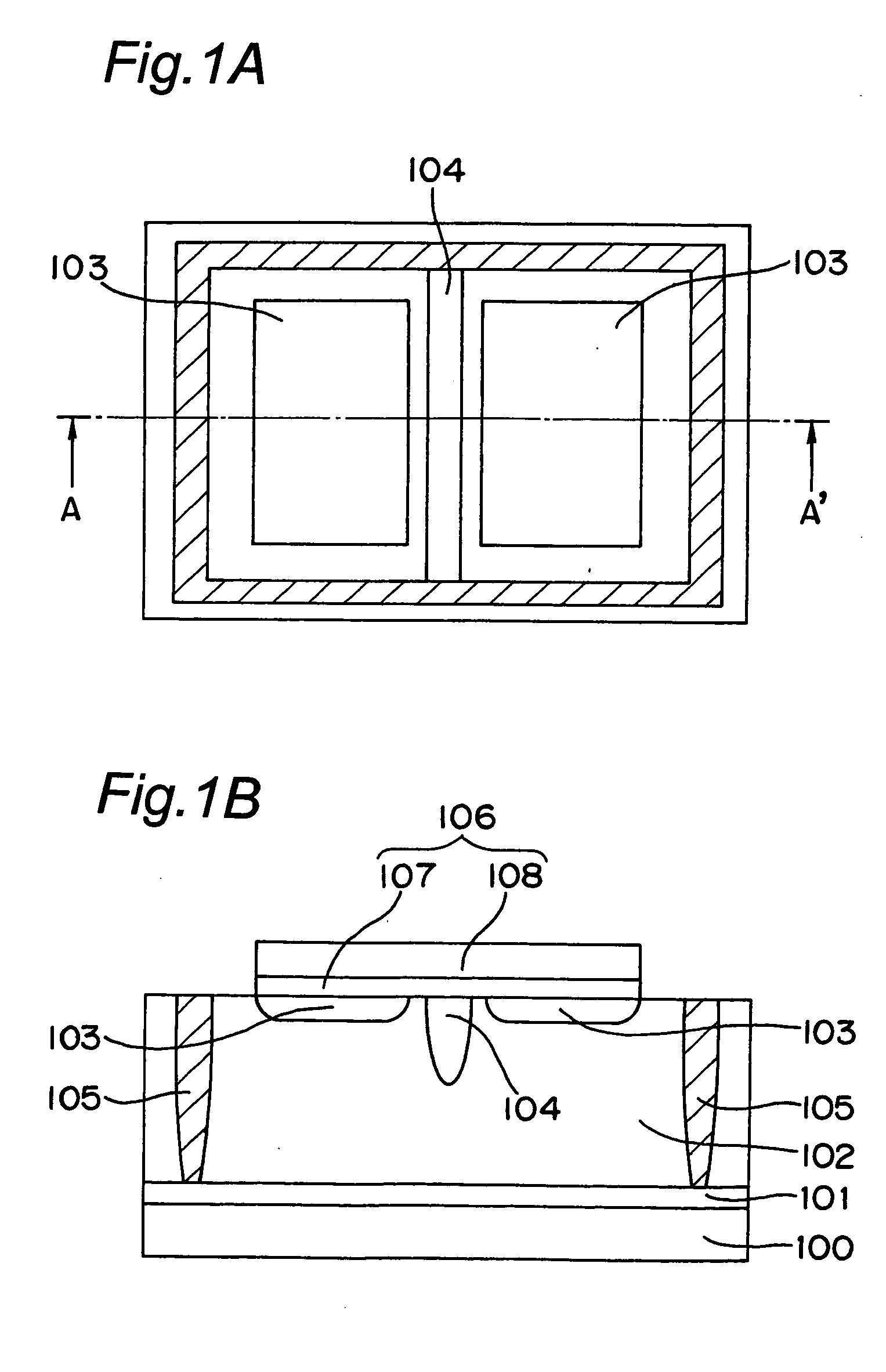
[0047]FIG. 1A and 1B are views of a light receiving device in the first embodiment of the present invention. FIG. 1A is a plan view showing the light receiving device while FIG. 1B is a cross sectional view taken along the arrow line A-A′ of FIG. 1A. This light receiving device is a split type light receiving device having a plurality of light receiving parts. In this embodiment, contacts, metal interconnections, interlayer insulating films and the like that are formed after a contact step are deleted.
[0048] The light receiving device includes a silicon substrate 100, a first P type diffusion layer 101 with impurity concentration of about 1E18 cm−3 and a thickness of about lam on the silicon substrate 100, and a P type semiconductor layer 102 with impurity concentration of about 1E13 to 1E16 cm−3 and a thickness of about 10 μm to 20 μm on the P type diffusion layer 101. On the surface part of the P type semiconductor layer 102, two N type diffusion layers 103 an...
second embodiment
THE SECOND EMBODIMENT
[0056]FIG. 3A is a plan view showing a light receiving device in the second embodiment of the present invention, while FIG. 3B is a cross sectional view taken along the arrow line B-B′ of FIG. 3A. In this embodiment, contacts, metal interconnections, interlayer insulating films and the like that are formed after a contact step are deleted.
[0057] The light receiving device of the present embodiment includes a silicon substrate 200, a first P type diffusion layer 201 with impurity concentration of about 1E18 cm−3 and a thickness of about 1 μm on the silicon substrate 200, and a P type semiconductor layer 202 with impurity concentration of about 1E13 to 1E16 cm−3 and a thickness of about 10 μm to 20 μm. On the surface part of the P type semiconductor layer 202, two N type diffusion layers 203 and 203 with impurity concentration of about 1E17 to 1E20 cm−3 in the vicinity of the top surface and a junction depth of about 0.2 μm to 1.5 μm are formed to constitute two ...
third embodiment
THE THIRD EMBODIMENT
[0063]FIG. 4A is a plan view showing a light receiving device in a third embodiment of the present invention, while FIG. 4B is a cross sectional view taken along the arrow line C-C′ of FIG. 4A.
[0064] The light receiving device includes a silicon substrate 300, a first P type diffusion layer 301 with impurity concentration of about 1E18 cm−3 and a thickness of about 1 μm on the silicon substrate 300, and a P type semiconductor layer 302 with impurity concentration of about 1E13 to 1E16 cm−3 and a thickness of about 10 μm to 20 μm on the first P type diffusion layer 301. On the surface part of the P type semiconductor layer 302, two N type diffusion layers 303 and 303 with impurity concentration of about 1E17 to 1E20 cm−3 in the vicinity of the top surface are formed to constitute light receiving parts. An impurity forming the N type diffusion layers 303 may be any element such as arsenic, phosphorus, and antimony as long as the element is pentavalent. It is to be...
PUM
 Abstract
Description
Claims
Application Information
 - R&D
- Intellectual Property
- Life Sciences
- Materials
- Tech Scout
- Unparalleled Data Quality
- Higher Quality Content
- 60% Fewer Hallucinations
Browse by: Latest US Patents, China's latest patents, Technical Efficacy Thesaurus, Application Domain, Technology Topic, Popular Technical Reports.
© 2025 PatSnap. All rights reserved.Legal|Privacy policy|Modern Slavery Act Transparency Statement|Sitemap|About US| Contact US: help@patsnap.com