
Phase shift mask blank, phase shift mask, and pattern transfer method

Active Publication Date: 2005-05-26
TOPPAN PHOTOMASK CO LTD +1
View PDF4 Cites 14 Cited by
  • Summary
  • Abstract
  • Description
  • Claims
  • Application Information

AI Technical Summary

Benefits of technology

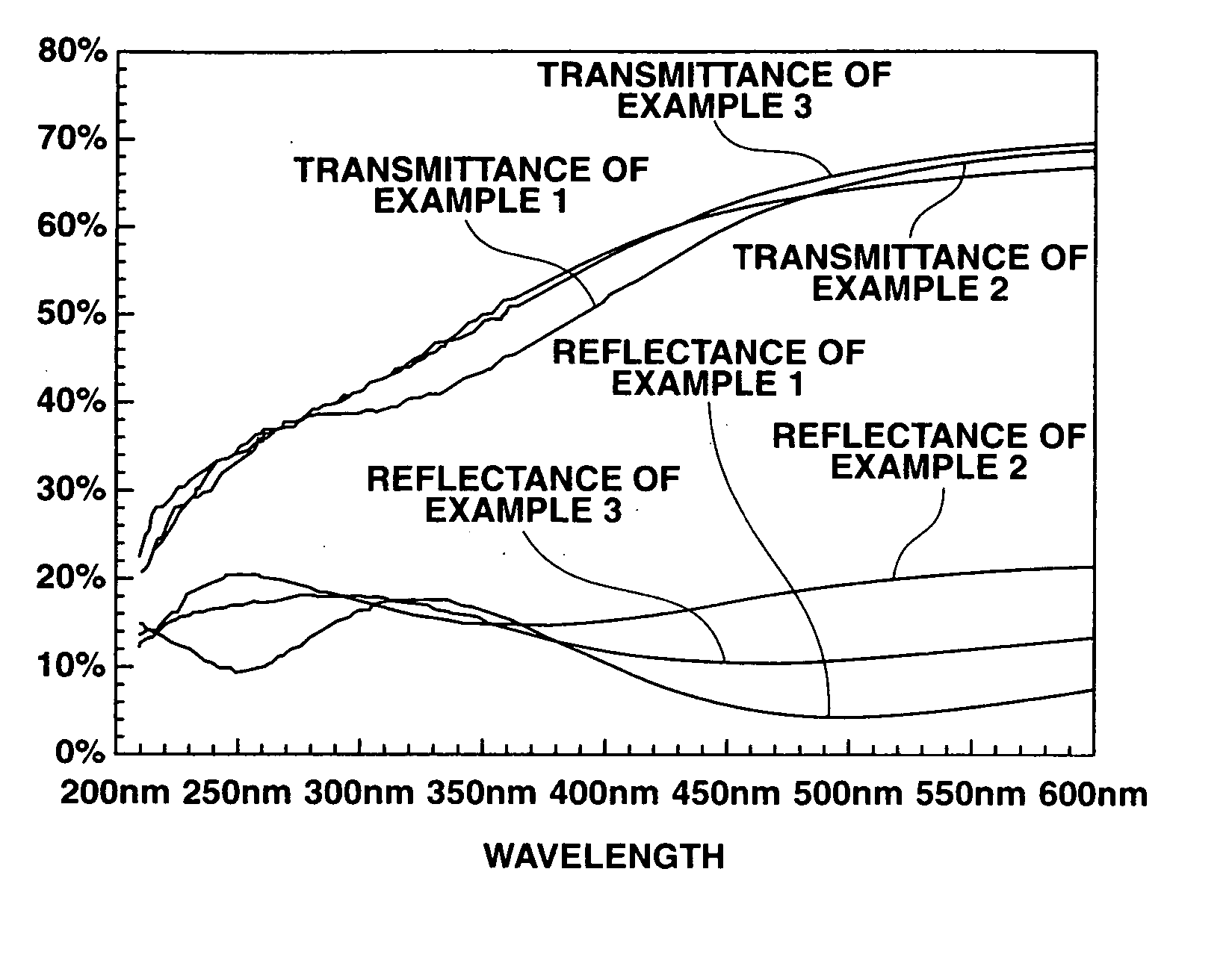
[0013] Therefore, an object of the present invention is to provide a phase shift mask blank which has minimized dependency of transmittance on wavelength and can be processed with a single dry etching gas; a phase shift mask using the same; and a pattern transfer method.
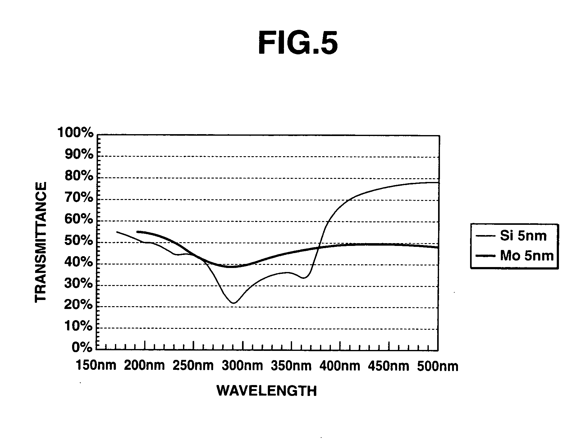
[0014] Regarding a phase shift mask blank comprising a phase shift multilayer film on a substrate, the inventor has discovered that when the phase shift multilayer film consists of at least one layer of light absorption function film formed of a metal or a metal and silicon, or an unsaturated metal compound in the form of an oxide, nitride, carbide, oxynitride, oxynitride carbide or nitride carbide comprising a metal or a metal and silicon as primary elements, and at least one layer of phase shift function film formed of an oxide, nitride, carbide, oxynitride, oxynitride carbide or nitride carbide comprising a metal or a metal and silicon, the light absorption function film has an extinction coefficient k relative to light of wavelength 157 to 260 nm which increases as the wavelength moves from 157 nm toward 260 nm, and the light absorption function film has a thickness of up to 15 nm, then this phase shift mask blank has minimized dependency of transmittance on wavelength and can be processed with a single dry etching gas.
[0015] When one layer of light absorption function film is present and disposed contiguous to the substrate, or when two layers of light absorption function film are present, and one of the two layers is disposed contiguous to the substrate, defects, if any, can be effectively repaired by means of a laser. When two layers of light absorption function film are present, the dependency of reflectance on wavelength can also be minimized. Then inspection becomes possible with a defect inspecting system of photo-detection type commonly employed in the mask manufacture process.
[0022] The phase shift multilayer film of the inventive phase shift mask blank has minimized dependency of transmittance on wavelength, can be processed with a single dry etching gas, and exhibits a favorable transmittance at both the exposure wavelength and the inspection wavelength. Thus the phase shift mask blank and the phase shift mask obtained therefrom according to the invention are amenable to the use of a shorter wavelength as the exposure wavelength.
[0023] When one layer of light absorption function film is disposed contiguous to the substrate, or when one of two layers of light absorption function film is disposed contiguous to the substrate, defects, if any, can be effectively repaired by means of a laser. The provision of two layers of light absorption function film also minimizes the dependency of reflectance on wavelength. Then inspection becomes possible with a defect inspecting system of photo-detection type commonly employed in the mask manufacture process.

Problems solved by technology

This lowers the process stability and adversely affects the manufacture yield of products.
Although the halftone type phase shift mask is an effective means for accomplishing a high resolution in a simple manner, it suffers from the following problem due to the difference between the wavelength at which light exposure through the mask is carried out (exposure wavelength) and the wavelength of light used for defect inspection of the mask itself (inspection wavelength).
The defect inspection system fails in inspection unless there is a contrast between the uncovered substrate area and the phase shifter.
If the transmittance of the phase shifter at the inspection wavelength exceeds 50%, its difference from the transmittance of the uncovered substrate area becomes too small to provide a sufficient contrast for inspection, interfering with defect inspection with a satisfactory precision.
The above-mentioned problem arising from the difference between the inspection wavelength and the exposure wavelength is pertinent not only to transmittance, but also to reflectance.
However, the prior art phase shift film of multilayer structure has a substantial difference in dry etching behavior between the transparent film having a phase shift function and the metal film having a light absorption function.
This necessitates a combination of etching processes using different etching gases in the mask manufacture, adding to the cost of mask manufacture (resulting from the increased expense of facility, an increased number of steps, and a reduced production yield).
Also, the halftone phase shift film of multilayer structure has the problem that it is impossible to reduce the dependency of transmittance and reflectance on wavelength at the same time.
In the structure in which a transparent film having a phase shift function is combined with a metal film having a light absorption function, a defect repairing system having a laser built therein operates so that the energy of laser light concentrates only in the film having a light absorption function, failing to provide satisfactory repair.

Method used


Image

  • Phase shift mask blank, phase shift mask, and pattern transfer method
  • Phase shift mask blank, phase shift mask, and pattern transfer method
  • Phase shift mask blank, phase shift mask, and pattern transfer method

Examples


example 1

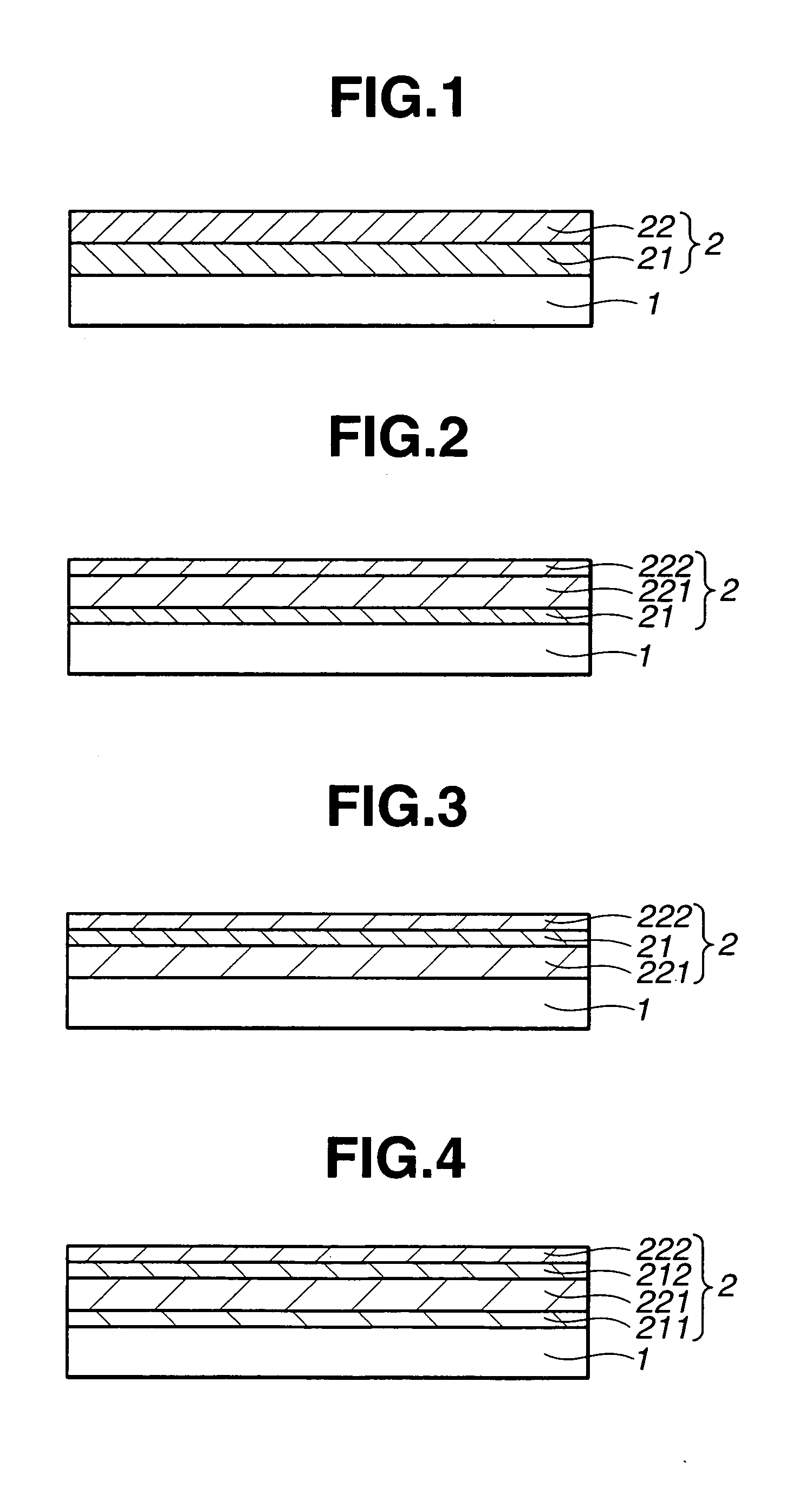
[0086] A phase shift mask blank having a phase shift multilayer film of three-layer structure deposited on a substrate as shown in FIG. 2 was prepared.

[0087] First, a light absorption function film was deposited on a quartz substrate. As the sputtering gas, Ar gas was fed at a flow rate of 15 cm3 / min. During the gas feed, a gas pressure of 0.15 Pa was set in the sputtering chamber. By applying a discharge power of 560 W across a sintered MoSi2 target and a discharge power of 1000 W across a Si single crystal target and rotating the substrate at 30 rpm, a film consisting of molybdenum and silicon (MoSi film) was deposited to a thickness of 2.5 nm, forming a light absorption function film. For the deposition, a d.c. sputtering system including two targets as shown in FIG. 13 was used (the same system was used in subsequent deposition). The system of FIG. 13 includes a chamber 101 in which a substrate 1 is rested on a rotating support 105, and a MoSi2 target 102a and a silicon target ...

example 2

[0097] A phase shift mask blank having a phase shift multilayer film of four-layer structure deposited on a substrate as shown in FIG. 4 was prepared.

[0098] The phase shift multilayer film was obtained by first depositing a first layer of light absorption function film on a quartz substrate under the same conditions as used for the light absorption function film in Example 1 except that the thickness was 1.25 nm, then depositing a first layer of phase shift function film under the same conditions as used in Example 1, depositing a second layer of light absorption function film under the same conditions as used for the first layer, and finally depositing a second layer of phase shift function film under the same conditions as used in Example 1.

[0099] The phase shift multilayer film was designed so as to provide a phase difference of 180° and a transmittance of 18% at a wavelength of 193 nm (ArF excimer laser).

[0100] The phase shift multilayer film of the thus obtained phase shift ...

example 3

[0106] A phase shift mask blank having a phase shift multilayer film of three-layer structure deposited on a substrate as shown in FIG. 3 was prepared.

[0107] The phase shift multilayer film was obtained by sequentially depositing a first layer of phase shift function film, a layer of light absorption function film, and a second layer of phase shift function film on a substrate in the described order. These layers were the same as the corresponding layers in Example 1 and deposited under the same conditions as in Example 1.

[0108] The phase shift multilayer film was designed so as to provide a phase difference of 180° and a transmittance of 18% at a wavelength of 193 nm (ArF excimer laser).

[0109] The phase shift multilayer film of the thus obtained phase shift mask blank was examined by the following tests.

Wavelength Dependency of Transmittance

[0110] The transmittance of the phase shift multilayer film was measured by the same procedure as in Example 1. The results are plotted i...


PUM


Abstract

In a phase shift mask blank comprising a phase shift multilayer film on a substrate, the phase shift multilayer film consists of at least one layer of light absorption function film and at least one layer of phase shift function film, and the light absorption function film has an extinction coefficient k which increases as the wavelength changes from 157 nm to 260 nm, and has a thickness of up to 15 nm. The phase shift mask blank has minimized wavelength dependency of transmittance and can be processed with a single dry etching gas.

Description

CROSS-REFERENCE TO RELATED APPLICATION [0001] This non-provisional application claims priority under 35 U.S.C. §119(a) on Patent Application No. 2003-364227 filed in Japan on Oct. 24, 2003, the entire contents of which are hereby incorporated by reference.TECHNICAL FIELD [0002] This invention relates to a phase shift mask blank and phase shift mask for use in the fabrication of semiconductor integrated circuits, and more particularly, to a phase shift mask of the halftone type wherein light of exposure wavelength is attenuated by the phase shift film, a phase shift mask blank from which the mask is obtained, and a pattern transfer method. BACKGROUND ART [0003] Photomasks are used in a wide variety of applications including the fabrication of semiconductor integrated circuits such as ICs, LSIs and VLSIs. Basically, the photomask is prepared from a photomask blank having a chromium based light-shielding film on a transparent substrate, by forming a predetermined pattern in the light-s...

Claims


Application Information

Patent Timeline
IPC IPC(8): G03F1/00G03F1/32G03F1/58G03F1/68H01L21/027
CPCG03F1/08G03F1/84G03F1/32G03F1/26
Inventor YOSHIKAWA, HIROKIINAZUKI, YUKIOOKAZAKI, SATOSHIHARAGUCHI, TAKASHIFUKUSHIMA, YUICHIII, YOSHIHIROSAGA, TADASHI
Owner TOPPAN PHOTOMASK CO LTD
Learn More