Microstructured substrates with profile-preserving organometallic coatings
a microstructured substrate and organometallic coating technology, applied in the direction of instruments, record information storage, transportation and packaging, etc., can solve the problems of general limited material scope, general knowledge of methods not suitable for producing cured polymeric coatings, and not particularly suited to coating substrates with microstructured profiles, etc., to achieve uniform surface properties and maintain uniformity
- Summary
- Abstract
- Description
- Claims
- Application Information
AI Technical Summary
Benefits of technology
Problems solved by technology
Method used
Image
Examples
example 1
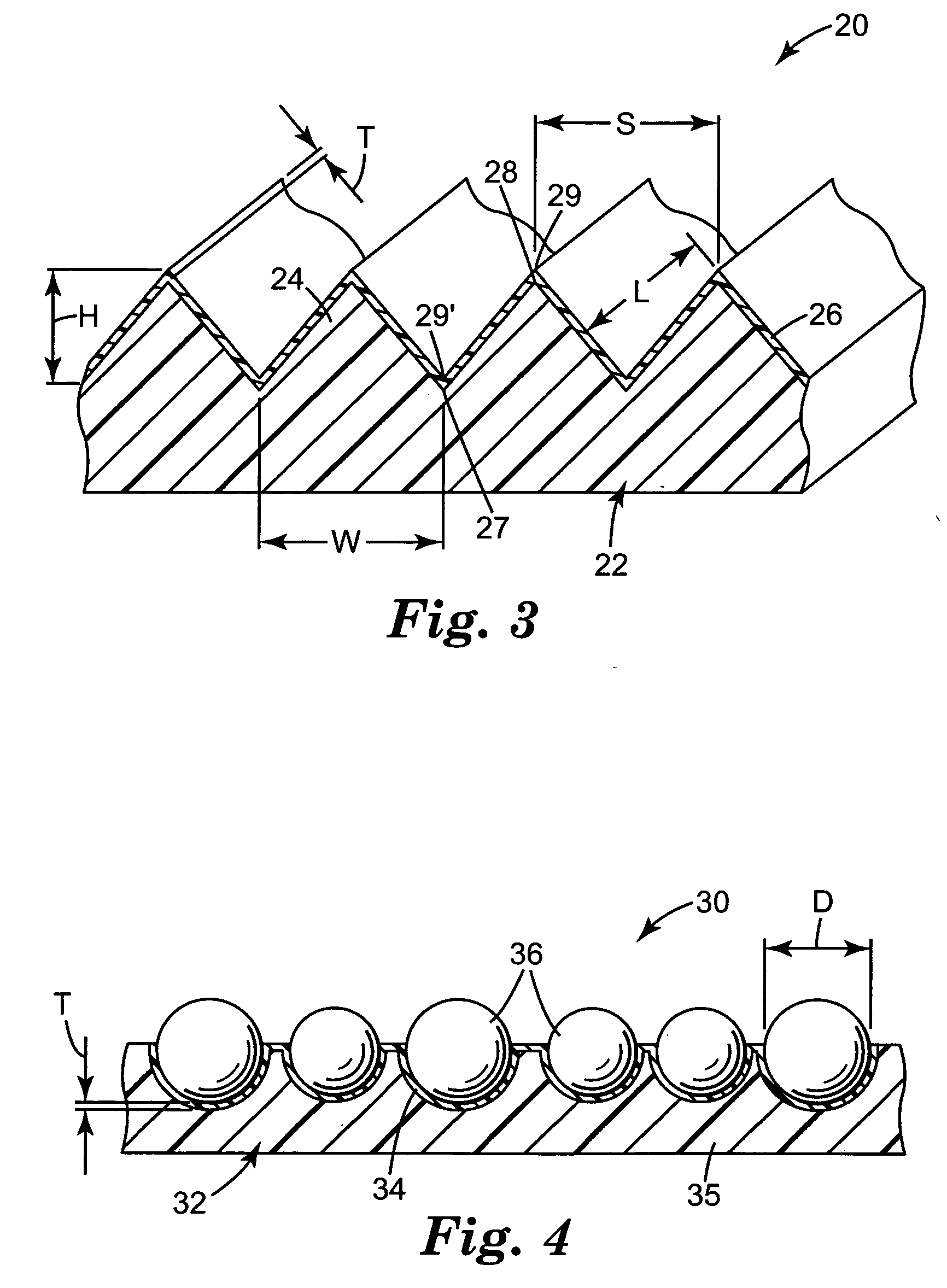
[0085] In this example, an article was produced that was constructed similar to the article 30 shown in FIG. 4. In producing this article, a temporary carrier sheet was provided that had a monolayer of glass microspheres (average diameter of about 60 μm and refractive index, 2.26) partially and temporarily embedded in the surface of a polyvinyl butyral resin crosslinked through its hydroxyl groups to a substantially thermoset state. The polyvinyl butyral resin was supported by a plasticized polyvinyl chloride coating on a paper carrier liner. This microstructured sheet of base material was referred to as wide-angle-flat-top (WAFT) beadcoat.
[0086] A sample of WAFT beadcoat was taped to a chilled steel drum of a monomer vapor deposition apparatus such as described in U.S. Pat. No. 4,842,893. The apparatus used a flash evaporation process to create a pre-polymer vapor that was coated using a vapor coating die. The vapor coating die directed the coating material onto the WAFT beadcoat....
example 2
[0089] Another piece of microstructured WAFT beadcoat, as described in Example 1, was taped to the chilled steel drum of the apparatus used in Example 1. For the monomer, a 50 / 50 by weight mixture of tris(2-hydroxyethyl) isocyanurate triacrylate and trimethylolpropane triacrylate was used at the same conditions given in Example 1, except that this mixture of monomers was heated to 80 ° C., the plasma power was at 1900 Watts and the chamber vacuum was at. 4.5×10⁻⁴ Torr. The deposited polymer thickness was estimated at approximately 6 μm. This is thinner than for Example 1, which used a lower molecular weight monomer as compared to the mixture of higher molecular weight monomers used in Example 2.
[0090] Aluminum metal was deposited in a bell jar vapor coater over the polymer coatings made in Examples 1 and 2 to form metal reflective layers that completed the optics for the enclosed-lens retroreflective sheeting. After applying the aluminum coating, a layer of pressure sensitive adhes...
example 3
[0094] Glass microspheres having an average diameter of 40 to 90 μm and a refractive index of 1.93 were partially embedded into a temporary carrier sheet, forming a microstructured substrate referred to as a beadcoat carrier. The beadcoat carrier was taped onto the chilled steel drum of the monomer vapor coating apparatus described in Example 1. Alternating layers of sec-butyl(dibromophenyl acrylate) (SBBPA), as described in International Publication WO 9850805 A1 (corresponding to U.S. patent application 08 / 853,998), and tripropylene glycol diacrylate (TRPGDA) were evaporated and condensed onto the beadcoat carrier while the chilled steel drum was maintained at −30° C. The drum rotated to move the sample past the plasma treater, vapor coating die, and electron beam curing head at a speed of 38 n / min. A nitrogen gas flow of 570 ml / min was applied to the 2000 Watt plasma treater. The room temperature tripropylene glycol diacrylate liquid flow was 1.2 ml / min, and the heated SBBPA liqu...
PUM
| Property | Measurement | Unit |
|---|---|---|
| diameter | aaaaa | aaaaa |
| thickness | aaaaa | aaaaa |
| thickness | aaaaa | aaaaa |
Abstract
Description
Claims
Application Information
 - R&D
- Intellectual Property
- Life Sciences
- Materials
- Tech Scout
- Unparalleled Data Quality
- Higher Quality Content
- 60% Fewer Hallucinations
Browse by: Latest US Patents, China's latest patents, Technical Efficacy Thesaurus, Application Domain, Technology Topic, Popular Technical Reports.
© 2025 PatSnap. All rights reserved.Legal|Privacy policy|Modern Slavery Act Transparency Statement|Sitemap|About US| Contact US: help@patsnap.com


