
Method of forming a recess channel trench pattern, and fabricating a recess channel transistor

a recess channel and trench pattern technology, applied in the field of recess channel trench pattern and recess channel transistor fabrication, can solve the problems of shortening the channel length, difficult control of influences, abnormal operation of the recess channel transistor, etc., and achieve the effect of avoiding residual substrate areas

Active Publication Date: 2005-04-14
SAMSUNG ELECTRONICS CO LTD
View PDF2 Cites 50 Cited by
  • Summary
  • Abstract
  • Description
  • Claims
  • Application Information

AI Technical Summary

Benefits of technology

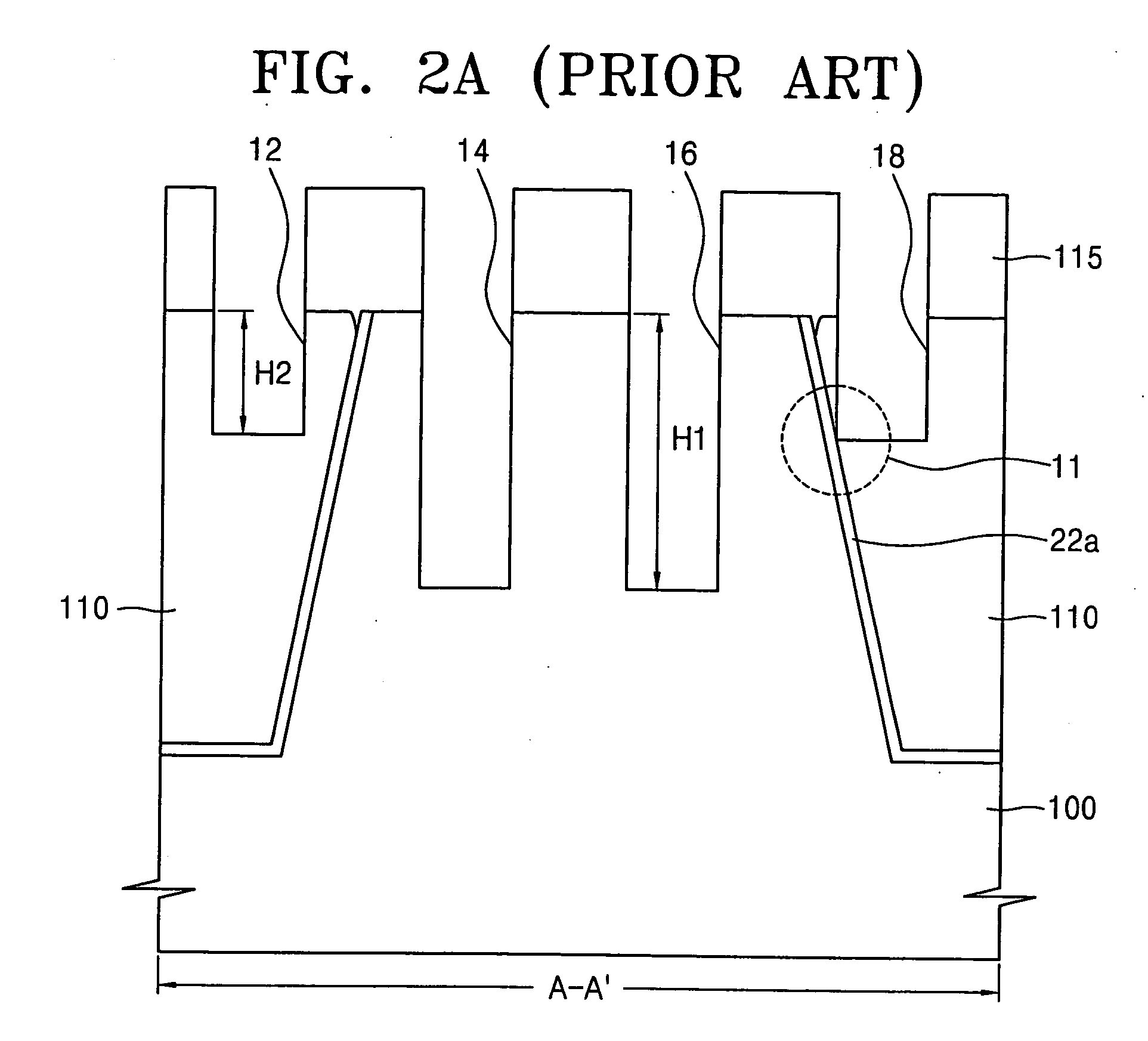
[0017] The present invention provides a method of forming a recess channel trench pattern capable of preventing a recess channel trench from intruding into a shallow trench isolation (STI) liner in a field region, thereby preventing a short between a recess gate and an active region and thoroughly avoiding residual substrate areas formed on both bottom sides of the recess channel trench.
[0018] The present invention also provides a method of fabricating a recess channel transistor capable of preventing a short between a recess gate and an active region, and thoroughly avoiding residual substrate areas formed on both bottom sides of the recess channel trench.

Problems solved by technology

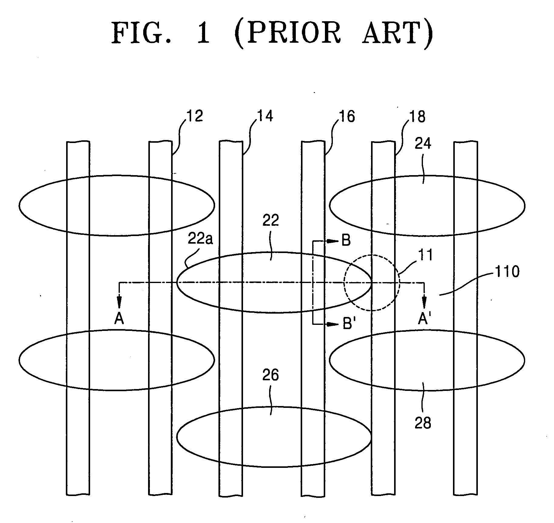
Lengths of channels are being shortened as a result of high integration density in semiconductor devices such as DRAMs, causing problems such as the short channel effect and punch through between source and drain regions, of which influences are difficult to control.
Even if the recess gate is not actually shorted, mutual interference caused as a result of making the recess channel trench 18 nearer to the substrate material 100 of the active region may bring about an abnormal operation of the recess channel transistor.
Thus, characteristics such as threshold voltage of the transistor are deteriorated.

Method used


Image

  • Method of forming a recess channel trench pattern, and fabricating a recess channel transistor
  • Method of forming a recess channel trench pattern, and fabricating a recess channel transistor
  • Method of forming a recess channel trench pattern, and fabricating a recess channel transistor

Examples


first embodiment

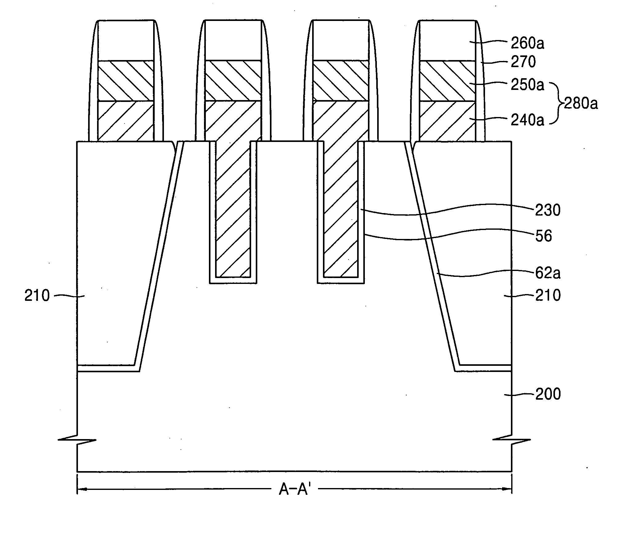
[0045]FIGS. 5A through 9B are sectional views showing a method of fabricating a recess channel transistor according to the present invention. The line A-A′ or B-B′ indicated by an arrow along the bottom portion of the figures denotes the respective drawing as a sectional view taken along line A-A′ or B-B′ of FIG. 4.

[0046] Referring to FIGS. 5A and 5B, a device isolating layer 210 with a STI structure is formed in a semiconductor substrate 200, thereby defining an active region and a field region. An impurity such as an n-type impurity with a conductivity opposite to that of the semiconductor substrate 200, is implanted to form source and drain regions (not shown) in the active region. A mask layer 215 is coated on the entire surface of the semiconductor substrate 200 including the device isolating layer 210. The mask layer 215 may be a photoresist layer or a hard mask layer such as a silicon nitride layer. When forming the device isolating layer 210, a STI liner 62a obtained by stac...

second embodiment

[0056]FIGS. 11A through 14B are sectional views showing a method of fabricating a recess channel transistor according to the present invention using the layout as shown in FIG. 10. Lines A-A′ and B-B′ designated in the bottom portion of the respective drawings indicate the respective sectional view taken along either lines A-A′ or B-B′.

[0057] Referring to FIGS. 11A and 11B, a mask layer pattern 315a is formed on a semiconductor substrate 300 formed with a device isolating layer 310 and source and drain regions (not shown) similar to those described with reference to FIGS. 6A and 6B. The mask layer pattern 315a is the isolated hole type as shown in FIG. 10. Accordingly, as shown in FIG. 11A when viewed from a section taken along line A-A′ of FIG. 10, the mask layer 315a is formed so the device isolating layer 310 is not exposed. Also, as shown in FIG. 11B when viewed from the section taken along line B-B′ of FIG. 10, the mask layer pattern 315a exposes the semiconductor substrate 300...

third embodiment

[0064]FIGS. 16A through 17B are sectional views showing a method of fabricating a recess channel transistor according to the present invention using the layout of FIG. 15. Lines A-A′ and B-B′ designated in the bottom portions of the respective drawings indicate the respective sectional view taken along either lines A-A′ or B-B′ of FIG. 15.

[0065] Referring to FIGS. 16A and 16B, a mask layer pattern 415a for defining a recess channel trench is formed on a semiconductor substrate 400 already formed with a device isolating layer 410, and source and drain regions (not shown). Using the mask layer pattern 415a as an etch mask, the exposed semiconductor substrate 400 and the device insulating layer 410 are anisotropically etched. At this time, an etch selectivity of the semiconductor substrate 400 material to the device isolating layer 410 is 1:1 or greater. For example, the etch selectivity may be 6:1 or greater. Since the etch selectivity of the semiconductor substrate 400 material is la...


PUM


Abstract

A method of forming a recess channel trench pattern for forming a recess channel transistor is provided. A mask layer is formed on a semiconductor substrate, which is then patterned to expose an active region and a portion of an adjacent device isolating layer with an isolated hole type pattern. Using this mask layer the semiconductor substrate and the device isolating layer portion are selectively and anisotropically etched, thereby forming a recess channel trench with an isolated hole type pattern. The mask layer may be patterned to be a curved line type. In this case, the once linear portion is curved to allow the device isolating layer portion exposed by the patterned mask layer to be spaced apart from an adjacent active region. The semiconductor substrate and the device isolating layer portion are then etched, thereby forming a recess channel trench with a curved line type pattern.

Description

BACKGROUND OF THE INVENTION [0001] This application claims the priority of Korean Patent Application No. 2003-70638, filed on Oct. 10, 2003, in the Korean Intellectual Property Office, the disclosure of which is incorporated herein in its entirety by reference. [0002] 1. Field of the Invention [0003] The present invention relates to a semiconductor integrated circuit device and a manufacturing method thereof, and more particularly to a recess channel transistor (RCT) used for a highly integrated semiconductor circuit, a method of fabricating the same, and a method of forming a recess channel trench pattern. [0004] 2. Description of the Related Art [0005] Lengths of channels are being shortened as a result of high integration density in semiconductor devices such as DRAMs, causing problems such as the short channel effect and punch through between source and drain regions, of which influences are difficult to control. Therefore, recess channel transistors are suggested for increasing...

Claims


Application Information

Patent Timeline
Patent Type & Authority Applications(United States)
IPC IPC(8): H01L29/78H01L21/28H01L21/336H01L21/8234H01L29/423H10B12/00
CPCH01L21/28123H01L21/823412H01L29/66621H01L27/10808H01L27/10876H01L21/823437H10B12/31H10B12/053H01L29/78
Inventor PARKKO, YONG-SUNAHN, TAE-HYUK
Owner SAMSUNG ELECTRONICS CO LTD
Learn More