
High density reagent array preparation methods

a high density, array technology, applied in chemical methods analysis, instruments, chemical indicators, etc., can solve the problems of limited usefulness of some arrays, difficult alignment of sippers with reagent spots, and reagent recovery, and achieve high and consistent reagent recovery, high density arrays, and high precision dissolution and recovery.

Inactive Publication Date: 2005-04-07
CAPLIPER LIFE SCI INC
View PDF5 Cites 34 Cited by
  • Summary
  • Abstract
  • Description
  • Claims
  • Application Information

AI Technical Summary

Benefits of technology

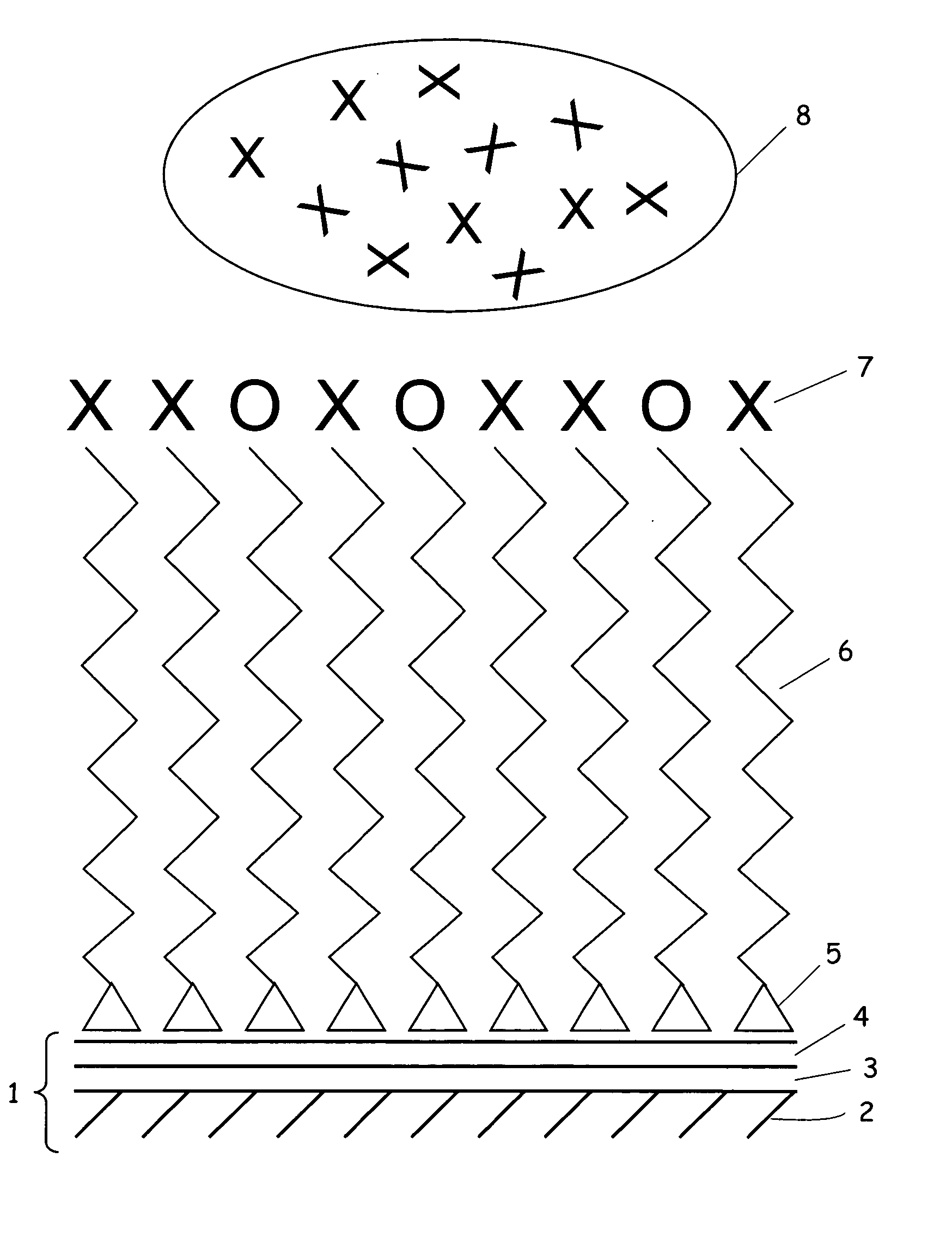
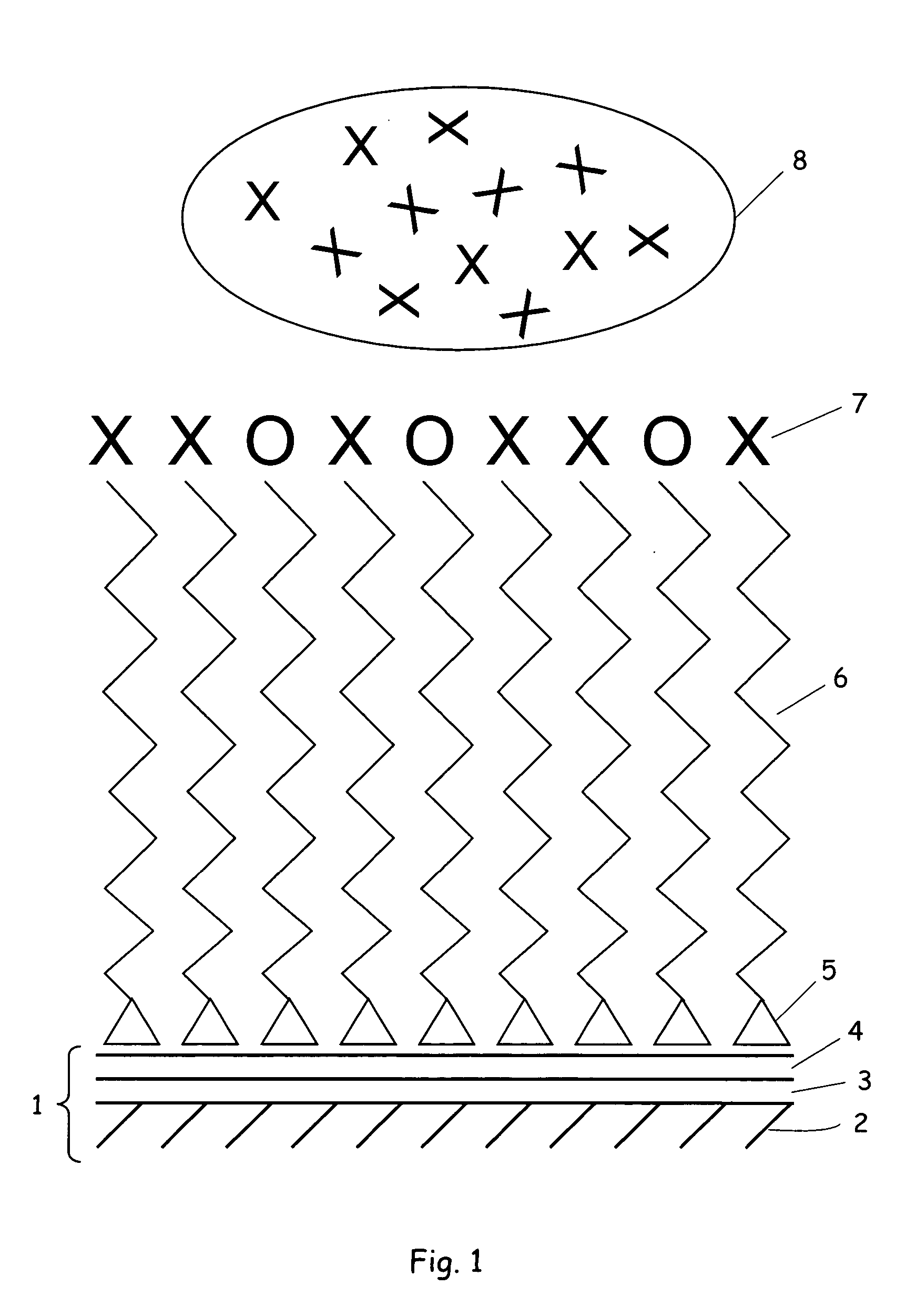
[0018] Embodiments of the present invention provide high-density array chips with self-assembled monolayer (SAM) surfaces to receive reagents. These SAM surfaces can be optimized for high and consistent recovery of reagents, and compatibility with reagents and solvents. SAM surfaces in accordance with the invention can provide high density arrays without cross-contamination. Reagent array chips in accordance with the invention can provide reagent spotting at high density without pre-alignment while providing high precision dissolution and recovery of reagents.
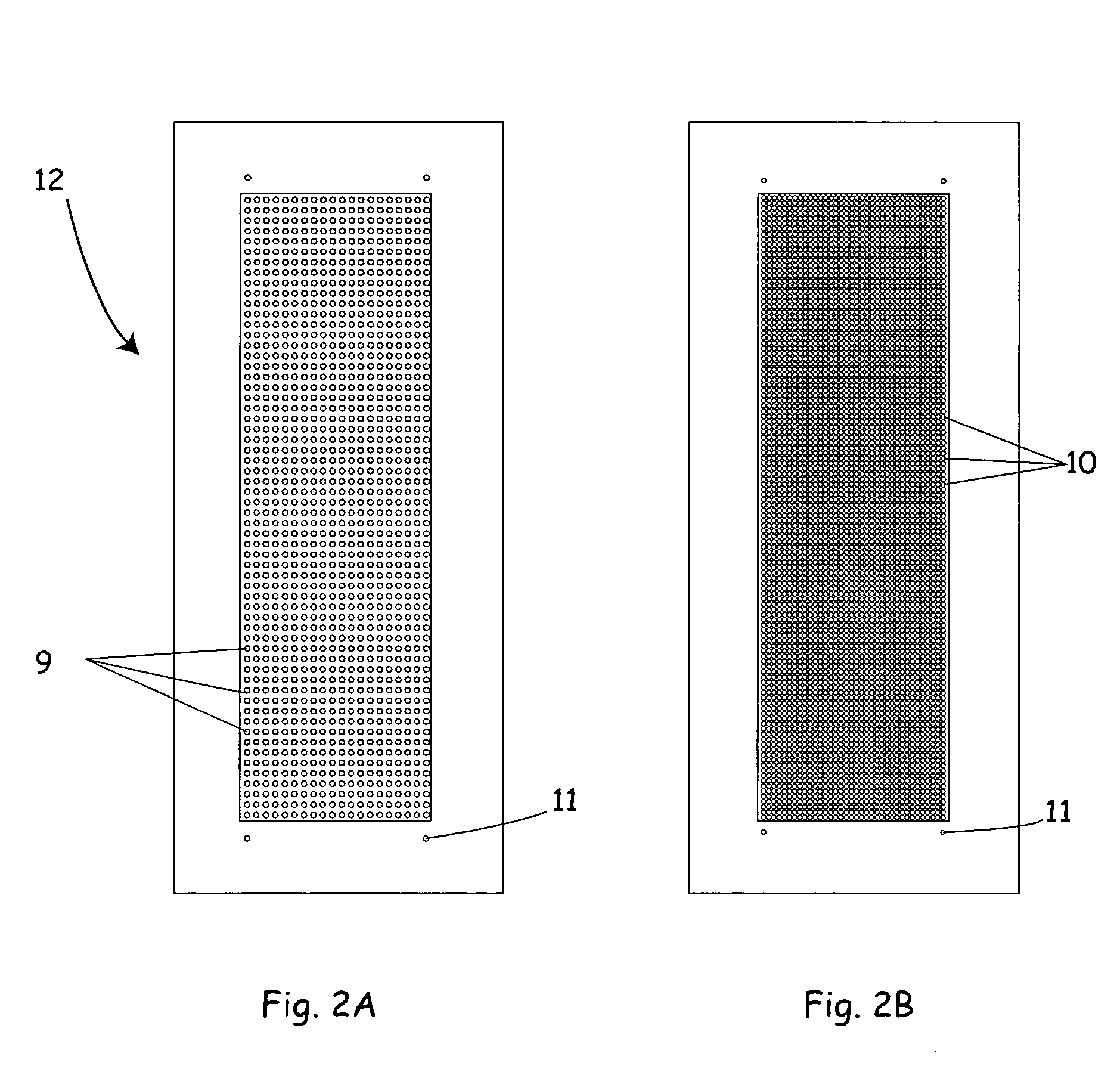
[0024] The SAM reagent arrays of the invention can provide very high density array spotting and recovery of reagents. Adjacent spotted reagent locations on array chips of the invention can be from 2 mm to about 0.9 mm, to about 0.5 mm, or less, as measured center to center.
[0028] The reagent arrays fabricated using methods of spotting reagents in accordance with the invention can include a protein, a nucleic acid, a cytokine, a receptor, a pharmaceutical, a virus, a buffer, a co-factor, a modulator, an inhibitor, an activator, a chemical, or a compound. Methods in accordance with the invention can provide SAMs with high and / or consistent recovery of desired reagents.
[0036] Reagent arrays in accordance with the invention can have patterned and / or unpatterned SAM regions formed by contacting one or more chip interfaces with a SAM formulation optimized to provide high and / or consistent recovery of the reagents from the library. The SAM formulation can be a solution and / or a vapor containing SAM molecules.
[0046] Embodiments of the present invention also provide methods of applying alignment marks onto reagent array chips. For example, an array of one or more reagents can be spotted onto a surface of the chip, an alignment mark composition can be applied to the surface in fixed register with the reagents, and the reagents and alignment mark composition can be dried to form one or more water insoluble substantially opaque alignment marks on the chip. The alignment mark composition can be applied concurrent with spotting the reagents. In such methods a collector (contact pin set or sipper) can be aligned with reference to one or more alignment marks, one or more dried reagents can be dissolved with a solvent, and the dissolved reagents can be collected from the chip by the collector to recover one or more reagents from the chip. The steps of spotting, applying, drying, aligning, dissolving, collecting, and / or transferring reagents can be effectively carried out using an automated instrument.

Problems solved by technology

The step of reagent recovery has many difficult aspects including the difficulty of locating reagent spots, preventing mixing of reagents in the dense array, obtaining high recovery of reagents, and obtaining consistent recovery of reagents.
These difficulties have placed a limit on the usefulness of some arrays and on the spotting density of array chips.
Alignment of the sippers with reagent spots can be difficult in a dense array.
On a dense array chip, application of recovery buffer can lead to cross contamination between spot locations.
As the reagents dry, they can contract off center or form jagged edges.
Poor alignment of sippers during recovery operations can compound buffer spreading.
Cross-contamination from wandering recovery buffers places a practical limit on array chip reagent spot density.
Broad spreading exposes reagents to a larger chip surface area where nonspecific adsorption of reagents can reduce the availability of some reagent elements.
Irregular and broad spreading provide less favorable mixing characteristics for the recovery buffer and less efficient dissolution.
Consistent reagent recovery can be a problem with current chip technologies.
These drying and adsorption irregularities can cause inconsistent recovery of reagents that adds a significant variable to experimental design and interpretation.
Broad and irregular spreading of spotted reagents can increase the dissolving time.
A slight increase in dissolution time per sample can add up to a significant time loss in the screening of a million reagents.
Inconsistent redissolution times of irregular spots can reduce the reproducibility of reagent recovery.
No single type of chip surface, such as metal, plastic, or glass, can prevent broad spreading of reagents in all solvents.
Broad spreading can make cross-contamination likely and reagent recovery difficult.
Reagent adsorption can also be a problem with various chip surfaces.
Where there is a high affinity between a reagent and a chip surface, recovery can be poor, and / or slow.
No single surface can provide an ideal low affinity characteristic for all types of reagents.
However, cleaning chips can be expensive, can introduce surfactant residues and does not address the irregularities inherent in glass surfaces.
Treatment of the chips with silanes can cover over irregularities of the glass surface, but may introduce new inconsistencies associated with amorphous and / or multilayer silane surfaces.

Method used


Image

  • High density reagent array preparation methods
  • High density reagent array preparation methods
  • High density reagent array preparation methods

Examples


example

[0134] The following non-limiting Example illustrates the use of surface coatings, consisting of self-assembled monolayers (SAM's) of alkanethiol molecules, to control the surface properties of a microarray substrate. X-ray photoelectron spectroscopy (XPS) and equilibrium contact angle measurements were performed in order to confirm the chemical content and wetability of these surface coatings. In order to test their performance in microarraying applications, sample microarrays were printed on these mixed alkanethiol films and then characterized with a non-contact visual metrology system and a fluorescence scanner. This Example demonstrates that utilizing mixed alkanethiol SAMs as a surface coating provides spatially homogeneous surface characteristics that are reproducible across multiple microarray substrates as well as within a substrate. In addition, this Example demonstrates that these films are stable and robust as they can maintain their surface characteristics over time. Ove...


PUM


Abstract

This invention provides reagent array chips having, e.g., reagents spotted at a high density onto self-assembled monolayers (SAMs) for consistent and high recovery. The invention teaches, e.g., methods to make and use reagent array chips to screen for protease substrates. Identified substrates can, e.g., then be used to screen for modulators of the protease activity and to establish quantitative assays for the protease.

Description

CROSS-REFERENCE TO RELATED APPLICATIONS [0001] This patent application is a continuation-in-part of U.S. patent application Ser. No. 10 / 630,357 filed Jul. 30, 2003, which claims the benefit of U.S. provisional patent application No. 60 / 400,458 filed Jul. 31, 2002, the entire contents of which are each incorporated by reference herein.FIELD OF THE INVENTION [0002] The invention is in the field of high-density array chips and methods to prepare and use such chips. Embodiments of the present invention relate to reagent array chips having a self-assembled monolayer (SAM) reagent spotting surface that provides consistent spotting and recovery of the reagents. Embodiments of the invention also provide patterned SAM surfaces on reagent chips and methods of spotting high-density reagent arrays. Method in accordance with the present invention includes methods of applying alignment marks to facilitate efficient and accurate determination of reagent spot locations on a high-density array chip....

Claims


Application Information

Patent Timeline
IPC IPC(8): G01N1/10
CPCB82Y15/00Y10T436/2575B82Y40/00B82Y30/00G01N1/28G01N1/10
Inventor DATWANI, SAMMY S.BIONDI, SHERRI A.VIJAYENDRAN, RAVIHORNING, TEXSONG, SHODANA
Owner CAPLIPER LIFE SCI INC
Learn More