Adhesion of copper and etch stop layer for copper alloy

a technology of etch stop layer and copper alloy, which is applied in the direction of semiconductor devices, electrical equipment, and semiconductor/solid-state device details, can solve the problems of increasing increasing the difficulty of using the interconnect metal for the creation of interconnects, and reducing the dielectric strength of the silicon dioxide layer, so as to achieve the effect of improving the adhesion

Inactive Publication Date: 2005-01-13
TAIWAN SEMICON MFG CO LTD
View PDF9 Cites 27 Cited by
  • Summary
  • Abstract
  • Description
  • Claims
  • Application Information

AI Technical Summary

Benefits of technology

[0016] A principal objective of the invention is to provide a copper interconnect of improved adhesion between the copper interconnect and an overlying cap layer of for instance etch stop material.

Problems solved by technology

In addition, the materials that are used for the creation of the interconnect metal, such as interconnect vias and interconnect traces, continues to present a challenge.
Copper from an interconnect may diffuse into a surrounding silicon dioxide layer, causing the dielectric to become conductive and decreasing the dielectric strength of the silicon dioxide layer.
Silicon nitride is frequently used as a diffusion barrier layer for copper, the disadvantage of this approach however is that metal interconnects preferably should not lie over a silicon nitride layer since the silicon nitride layer has a high dielectric constant when compared with silicon dioxide, causing an undesirable increase in the capacitance between the interconnect metal and the underlying substrate.
Copper is also known to have low adhesive strength to various insulating layers and is difficult to pattern by masking and etching a blanket layer of copper in order to create intricate structural circuit elements.

Method used


Image

  • Adhesion of copper and etch stop layer for copper alloy
  • Adhesion of copper and etch stop layer for copper alloy
  • Adhesion of copper and etch stop layer for copper alloy

Examples


Embodiment Construction

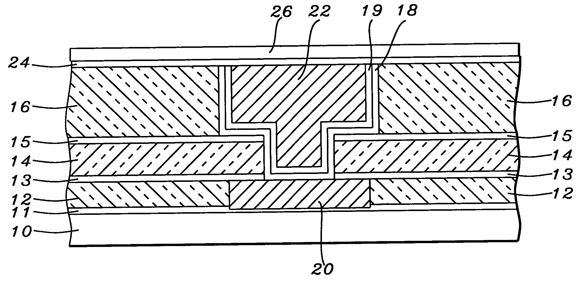
[0028] Copper, as previously stated, suffers from high diffusivity in common insulating materials such as silicon oxide and oxygen-containing polymers. For instance, copper tends to diffuse into polyimide during high temperature processing of the polyimide.

[0029] This causes severe corrosion of the copper and the polyimide due to the copper combining with oxygen in the polyimide. This corrosion may result in loss of adhesion, delamination, voids, and ultimately a catastrophic failure of the component. Copper interconnects are therefore conventionally encapsulated in at least one diffusion barrier to prevent diffusion into the surrounding layer of dielectric such as a layer of silicon dioxide.

[0030] A typical barrier layer is formed using rf sputtering of titanium nitride, tantalum, tungsten, niobium, molybdenum, Ti / TiN or Ti / W and is more preferably formed using TiN. The barrier layer can also be used to improve the adhesion of a subsequent overlying tungsten layer. A barrier laye...


PUM


Abstract

A new method and structure is provided for the creation of a copper dual damascene interconnect. A dual damascene structure is created in the layer of dielectric, optionally a metal barrier layer is deposited over exposed surfaces of the dual damascene structure. A copper seed layer is deposited, the dual damascene structure is filled with copper. An anneal is applied to the created copper interconnect after which excess copper is removed from the dielectric. Of critical importance to the invention, a thin layer of oxide is then deposited as a cap layer over the copper dual damascene interconnect, an etch stop layer is then deposited over the thin layer of oxide for continued upper-level metallization.

Description

RELATED PATENT APPLICATION [0001] This application is related to Ser. No. 10 / 361,732 (TS01-1676), filed on Feb. 10, 2003, and to Ser. No. 10 / 350,837 (TS02-338) filed on Jan. 24, 2003, assigned to common assignee.BACKGROUND OF THE INVENTION [0002] (1) Field of the Invention [0003] The invention relates to the fabrication of integrated circuit devices, and more particularly, to a method of improving copper interconnect reliability performance by improving the adhesion between the copper of the copper interconnect and a barrier layer. [0004] (2) Description of the Prior Art [0005] Performance improvements of Integrated Circuits are typically achieved by device miniaturization, which concurrently results in increasing the packaging density of the created Integrated Circuits. Methods and materials that are applied for interconnecting Integrated Circuits are therefore becoming an increasingly more importance part of creating packaged semiconductor devices. [0006] The selection of insulati...

Claims


Application Information

Patent Timeline
IPC IPC(8): H01L21/44H01L21/4763H01L21/768H01L23/532H01L33/00
CPCH01L21/76807H01L21/76831H01L21/76832H01L21/76834H01L23/53295H01L21/76855H01L21/76864H01L21/76873H01L23/53238H01L21/76843H01L2924/0002H01L2924/00
Inventor LIN, JING CHENGHSIEH, CHING-HUASHUE, SHAU-LINLIANG, MONG-SONG
Owner TAIWAN SEMICON MFG CO LTD
Why Eureka
Try Eureka