Semiconductor device and manufacturing method for same

a technology applied in the field of semiconductor devices and manufacturing methods for same, can solve problems such as preventing reliable communication, abnormal operation of devices, interference in device communication, etc., and achieves good shielding characteristics, improved shielding effect, and increased sensitivity

Inactive Publication Date: 2004-09-09
SHARP KK
View PDF9 Cites 3 Cited by
  • Summary
  • Abstract
  • Description
  • Claims
  • Application Information

AI Technical Summary

Benefits of technology

[0014] In accordance with one or more embodiments of the present invention, a semiconductor device in which one or more semiconductor chips have been mounted onto one or more substrates incorporating patterned wiring and the entirety has been sealed with one or more resins is such that one or more electrically conductive patterns for shielding is or are formed at one or more end faces at the top of at least one of the substrate or substrates. Here, at least one of the electrically conductive pattern or patterns may formed from copper foil. In this way, by forming electrically conductive pattern(s) for shielding at end face(s) at top(s) of substrate(s) and attaching such electrically conductive pattern(s) at region(s) of ground plane pattern(s) on circuit board(s) of apparatus(es) which is or are provided with such semiconductor device(s), it is possible to shield semiconductor device(s) even without use of shield case(s). In such case, by applying material(s) possessing good shielding characteristics, e.g., gold plating, over copper foil, it is possible to increase sensitivity with respect to electromagnetic noise and improve shielding effect (anti-electromagnetic-noise effect).
[0015] Furthermore, one or more shield cases may be attached over at least one of the electrically conductive pattern or patterns by way of one or more intervening electrically conductive adhesives. In such a case, at least one surface of at least one of the shield case or cases may be plated with gold. This will permit further improvement in shielding effect. Furthermore, application of gold plating will make it possible to prevent occurrence of degradation in characteristics due to the effects of contact resistance and / or occurrence of solder defects due to copper foil surface oxidation.
[0016] Furthermore, in the event that gold plating is applied to shield case(s), and / or in the event that gold plating is applied to electrically conductive pattern(s), silver paste may be applied to electrically conductive pattern(s) before attaching shield case(s). Due to compatibility between silver paste and gold plating, this makes it possible to improve adhesive strength.

Problems solved by technology

However, regardless of the product in question, the device is never used on its own, infrared communication instead being but one function which is always incorporated into some apparatus or the other.
That is, because the infrared communication device is installed within an apparatus, the problem has existed that communications carried out by the device can be affected by interference due to electromagnetic noise which is generated by the apparatus itself and / or electromagnetic noise from the exterior (e.g., mobile telephones, household appliances, and other such products which generate electromagnetic waves, and so forth).
Thus, the trend toward reduced infrared communication device size has in fact caused decreased resistance to electromagnetic noise as result of elimination of the shield case despite the fact that there is more need than was the case conventionally to increase resistance to electromagnetic noise, resulting in abnormal operation of the device and preventing reliable communication.
Especially with the recent increases in data communication speeds, the effects of noise can no longer be ignored.
Furthermore, whereas the presence of the shield case had conventionally provided some basis for acceptable antinoise characteristics, the recent proliferation of mobile telephones has brought a further steady worsening of the environment with respect to electromagnetic noise, to the point where the mere inclusion of a shield case can no longer be considered to be a completely acceptable strategy.
Furthermore, where a shield case had been provided, in the device disclosed at the aforementioned Japanese Patent Application Publication Kokai No. 2001-127310--like the infrared communication device shown in FIG. 9--the shield case was merely attached by adhesive to the device, the absence of any provision for establishing electrical continuity with the device necessitating that terminal(s) be provided for connecting to ground.
And this has resulted in the problem that it has caused the device itself to increase in size.
Furthermore, with respect to the other strategy for dealing with electromagnetic noise, i.e., adoption of a constitution in which electromagnetic-noise-resisting circuitry is added to the IC circuitry, because this causes considerable increase in the number of circuit elements as well as increased IC chip surface area, the concomitant increase in cost and increase in device dimensions have been problems.
But decreased diameter at through-holes 102 has placed demands on dicing precision, such that in practice any displacement and / or stresses resulting therefrom has caused disappearance of terminals and / or peeling of copper foil from the end face thereof, resulting in defective product and leading to increases in cost due to lowered yield.

Method used


Image

  • Semiconductor device and manufacturing method for same
  • Semiconductor device and manufacturing method for same
  • Semiconductor device and manufacturing method for same

Examples


Embodiment Construction

[0031] Below, embodiments of the present invention are described with reference to the drawings.

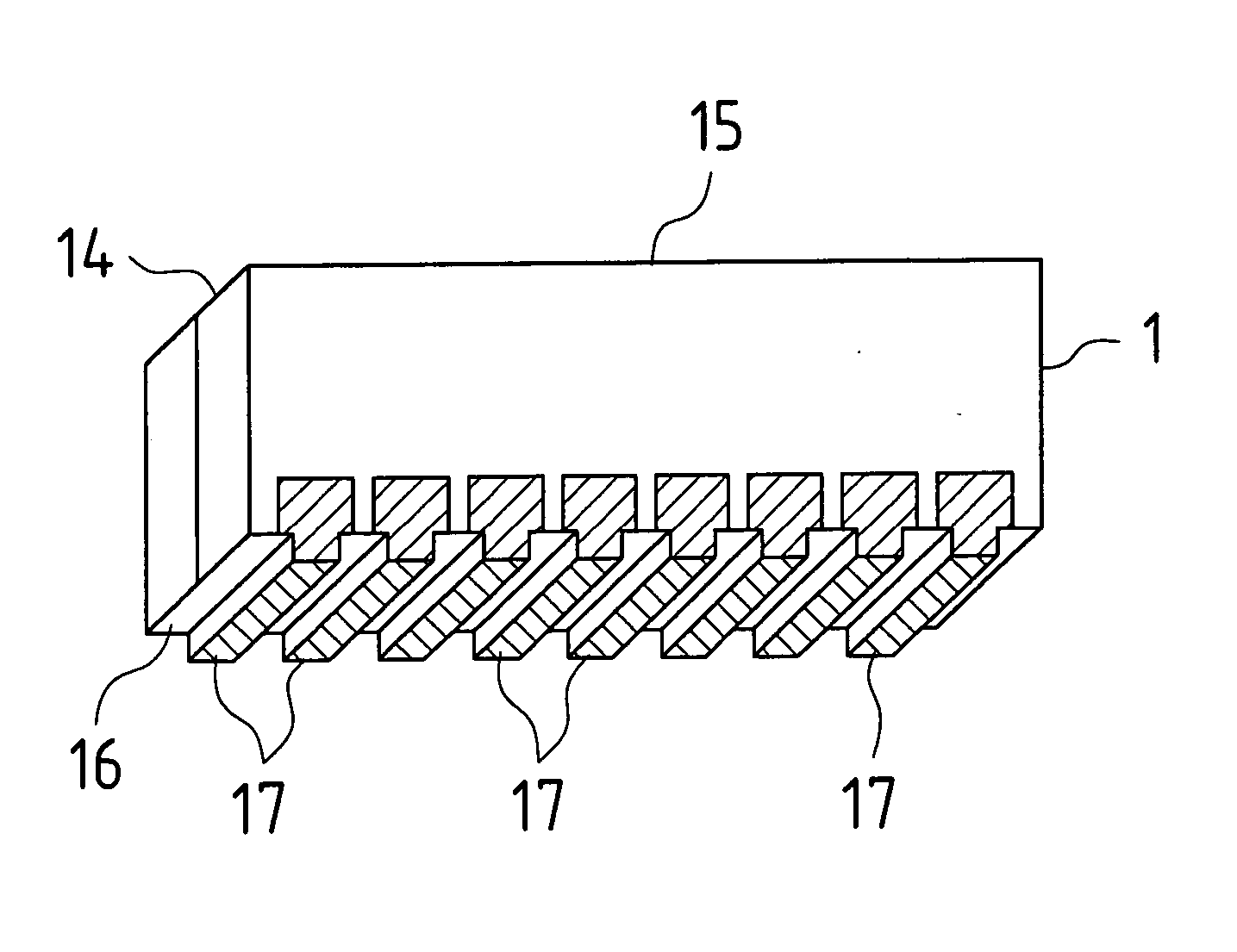
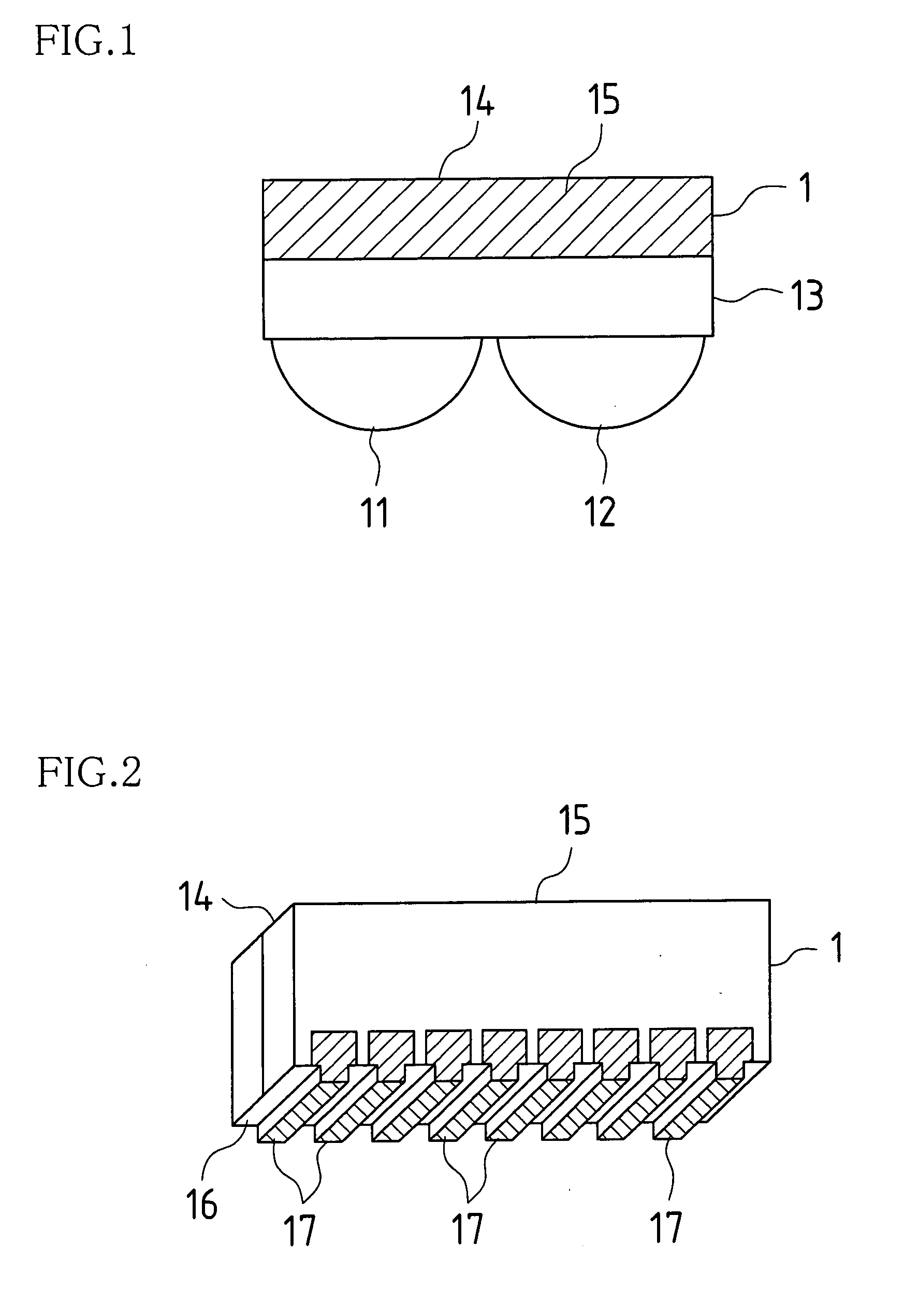
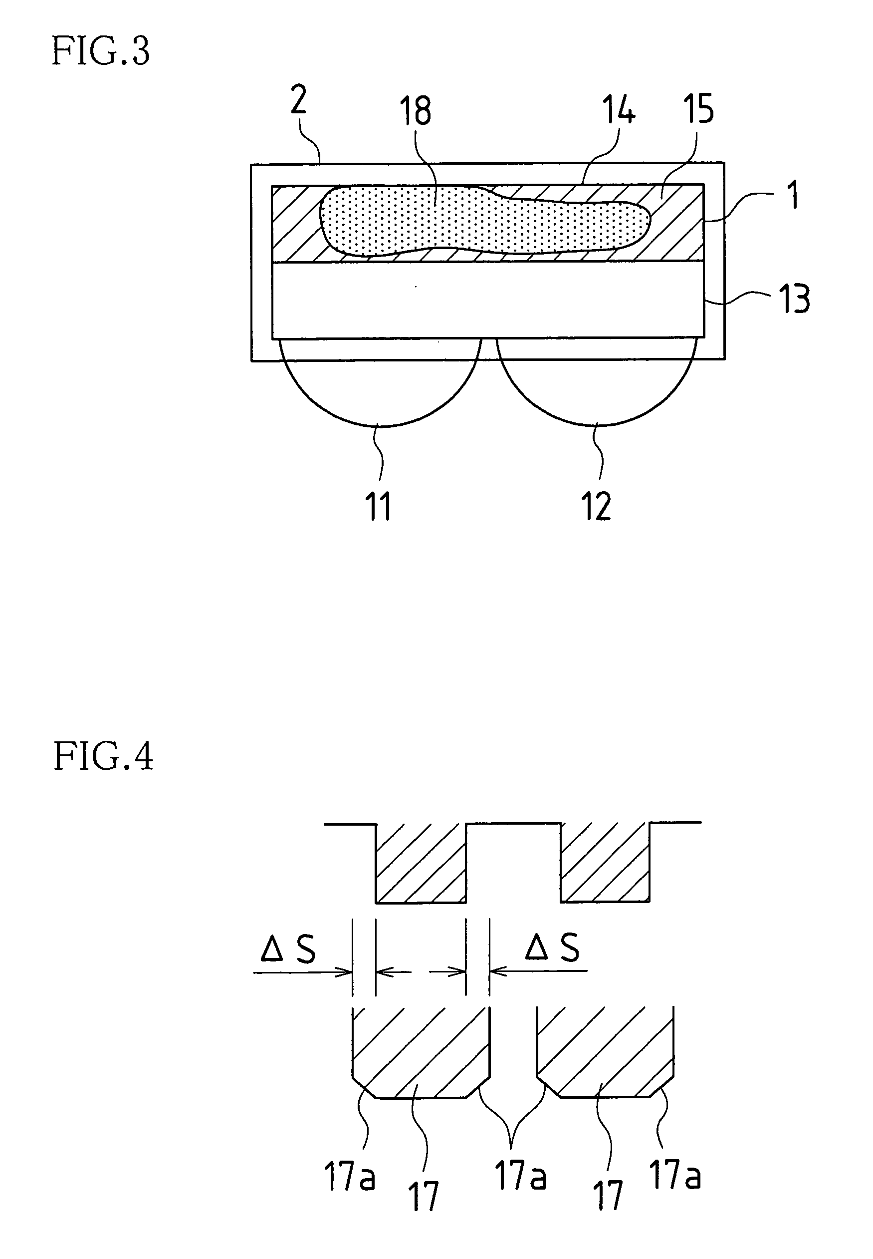
[0032] FIGS. 1 and 2 are drawings showing the external appearance of a semiconductor device in accordance with the present invention, FIG. 1 being a plan view of the semiconductor device as viewed from above, and FIG. 2 being an oblique view of the bottom of the semiconductor device as viewed from the back.

[0033] In forming this semiconductor device, substrate(s) 1--patterned wiring, not shown, being formed thereon--is furnished with light emitting diode chip(s), photodiode chip(s), IC chip(s), and / or other such chip(s), not shown; these are mounted thereon by means of die bonding, wire bonding, and / or the like; and molded resin(s) 13 is or are thereafter applied to the entirety thereof together with light-emitting lens portion(s) 11 and light-receiving lens portion(s) 12. In addition, in the present embodiment, the manufacturing method described below is employed to form electrically con...


PUM


Abstract

A semiconductor device in which semiconductor chip(s) is or are mounted onto substrate(s) incorporating patterned wiring and the entirety or entireties has or have been sealed with resin(s), wherein by forming electrically conductive pattern(s) for shielding at end face(s) at top(s) of substrate(s) and attaching such electrically conductive pattern(s) to region(s) of ground plane pattern(s) on circuit board(s) of apparatus(es) which is or are provided with such semiconductor device(s), it is possible to shield semiconductor device(s) even without use of shield case(s). In such case, by applying material(s) possessing good shielding characteristics, e.g., gold plating, over electrically conductive pattern(s), it is possible to increase sensitivity with respect to electromagnetic noise and improve shielding effect (anti-electromagnetic-noise effect).

Description

BACKGROUND OF INVENTION[0001] This Nonprovisional application claims priority under 35 U.S.C. .sctn.119(a) on patent Application No. 2003-060083 filed in Japan on Mar. 6, 2003, the entire contents of which are hereby incorporated by reference.[0002] The present invention pertains to a semiconductor device that may be used for sensors and / or for data communications which make use of light, and to a manufacturing method for same. More particularly, the present invention pertains to a semiconductor device that may be used in an infrared communication device, and to a manufacturing method for same.[0003] Referring to FIG. 7, a manufacturing method for a conventional semiconductor device, e.g., an infrared communication device, will be described.[0004] First, substrate 101 is prepared, a plurality of fields containing patterned wiring, not shown, being formed horizontally and vertically thereon; light emitting diode chips, photodiode chips, IC chips, and / or other such semiconductor chips...

Claims


Application Information

Patent Timeline
Patent Type & Authority Applications(United States)
IPC IPC(8): H05K9/00H01L23/00H01L23/498H01L23/552H01L31/02H01L33/48H01L33/54H01L33/56H01L33/62H04B10/11H04B10/2507H04B10/40H04B10/50H04B10/60H04B10/67
CPCH01L23/49805H01L2924/12041H01L24/97H01L2924/01004H01L2924/01005H01L2924/01029H01L2924/01033H01L2924/01047H01L2924/01078H01L2924/01079H01L2924/01082H01L2924/14H01L2924/3025H01L2924/01006H01L23/552H01L2924/181H01L2924/12043H01L2924/00
Inventor TAKASE, KENJI
Owner SHARP KK
Why Eureka
Try Eureka