
Method of producing ceramic multilayer substrate

a multi-layer substrate and ceramic technology, applied in the direction of structural fixed capacitor combination, cell components, electrochemical generators, etc., can solve the problems of substrate deflection, cracking or distorted, and it is impossible according to this production method to adjust the resistance or capacitance of the resistor or capacitor

Active Publication Date: 2004-07-29
MURATA MFG CO LTD
View PDF6 Cites 32 Cited by
  • Summary
  • Abstract
  • Description
  • Claims
  • Application Information

AI Technical Summary

Benefits of technology

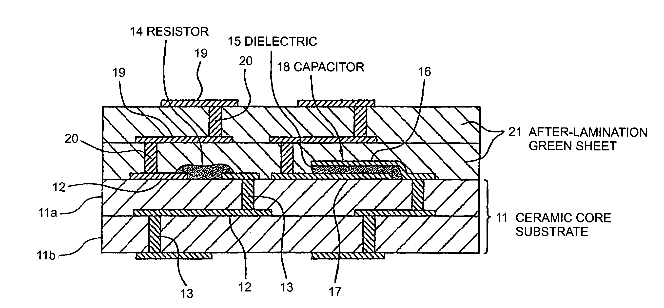
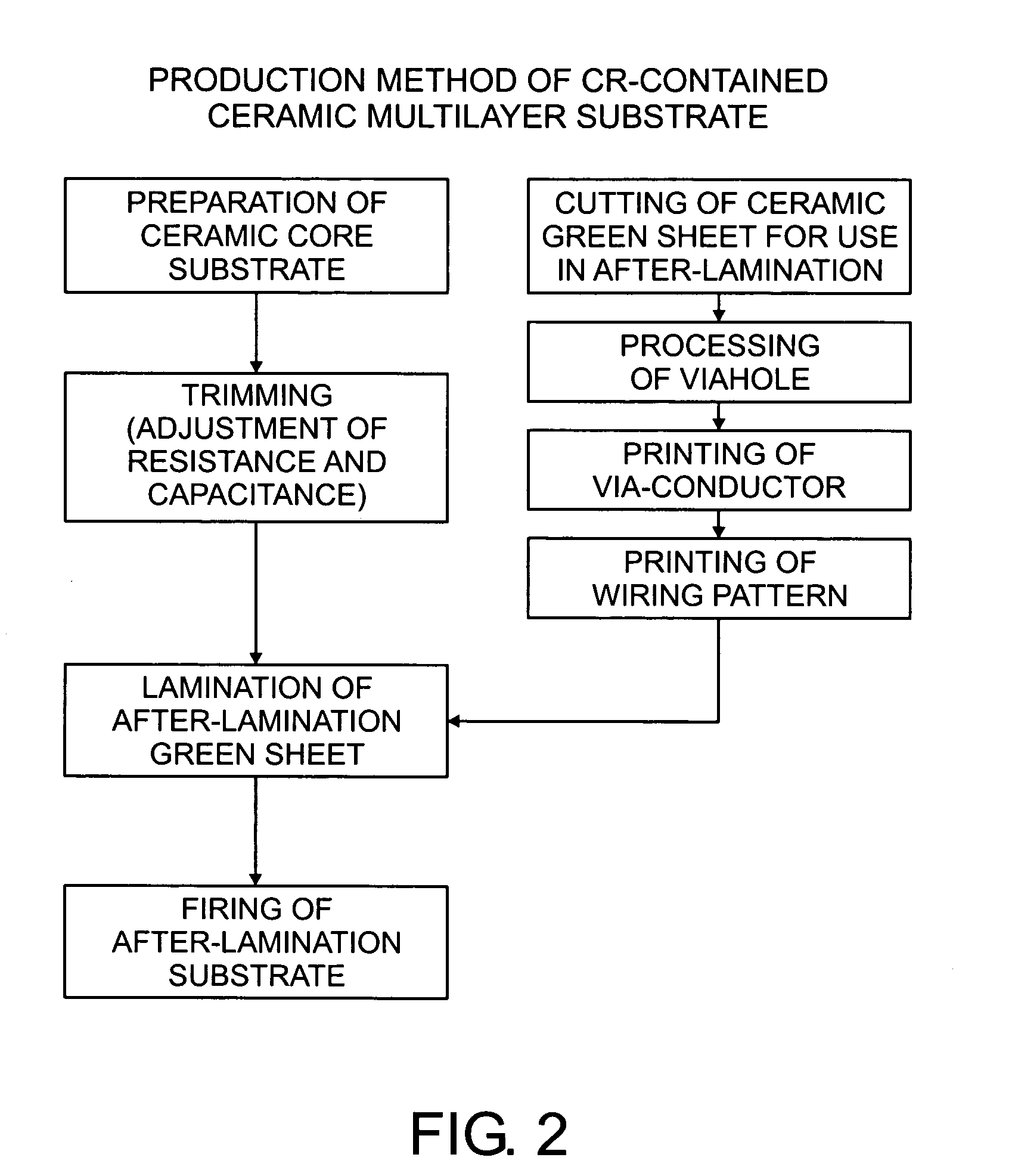
[0014] According to the method of producing a ceramic multilayer substrate of the present invention, after the resistor and the capacitor are fired simultaneously with the ceramic core substrate, or the resistor and the dielectric and electrodes of the capacitor are printed on the fired ceramic core substrate to be fired, the resistor and the capacitor are trimmed so that the resistance and the capacitance are adjusted. Thus, the resistance and the capacitance can be adjusted with high precision by trimming before the lamination. Thereafter, at least one after-lamination green sheet is laminated onto the surface of the ceramic core substrate. Thus, the after-lamination substrate is formed. The after-lamination substrate is fired at a temperature lower than the sintering temperature of the resistor and the dielectric. Thus, the sintered resistor and dielectric can be prevented from being softened and melted when the after-lamination substrate is fired. Moreover, the sintering states of the resistor and the dielectric can be prevented from being changed. The resistance and the capacitance accurately adjusted by trimming before the after-lamination substrate is fired (before the after-lamination green sheet is laminated) can be kept as they are, and not be changed by the firing. Thus, the ceramic multilayer substrate containing the resistor and the capacitor is a high quality one, and has less variations of the resistance and the capacitance.
[0015] Preferably, the firing temperature of the after-lamination substrate is set at a temperature which is lower than the glass yield point of a glass component contained in the resistor and / or the dielectric of the capacitor. Thereby, the sintered resistor and dielectric can be securely prevented from being softened and melted when the after-lamination substrate is fired. Thus, the dispersions of the resistance and the capacitance, which may be caused by the firing, can be securely reduced.
[0016] Also, preferably, the after-lamination green sheet is made from a SiO.sub.2--Al.sub.2O.sub.3--CaO--B.sub.2O.sub.3--Li.sub.2O type glass. The SiO.sub.2--Al.sub.2O.sub.3--CaO--B.sub.2O.sub.3--Li.sub.2O type glass has a glass yield point of 620.degree. C. Thus, the after-lamination substrate can be fired at a lower temperature (e.g., 700.degree. C.) compared to the glass yielding points of the resistor and the dielectric which contain a different glass. The variation of the resistance and the capacitance, which may be caused by firing, can thereby be securely reduced.
[0017] Also, preferably, the ceramic core substrate is made from a low-temperature firing ceramic which is fired at a temperature of about 800.degree. C. to 1000.degree. C. Thereby, advantageously, the ceramic core substrate, the resistor and the capacitor can be simultaneously fired. The number of firing processes can be reduced. In addition, as a wiring conductor which is fired simultaneously with the ceramic core substrate, metals with low melting points such as Ag type conductors having a low resistance and superior electrical characteristics can be employed. Needless to say, the resistor and the dielectric and electrodes of the capacitor may be printed on the fired ceramic core substrate and then fired in the case in which the ceramic core substrate is made from a low temperature firing ceramic.
[0019] As a countermeasure against the above-described problems, the ceramic core substrate may be formed to have a multilayer structure. Thus, the mechanical strength of the ceramic core substrate can be enhanced so that the distortion of the fired substrate is eliminated with the wiring-density of the ceramic core substrate being enhanced and also with the size being reduced.
[0020] Moreover, preferably, a constraining green sheet incapable of being sintered at the sintering temperature of the after-lamination green sheet is laminated onto the after-lamination green sheet laminated as the outermost layer of the after-lamination substrate. In the subsequent firing step, the after-lamination green sheet is constraininglyfired at the sintering temperature thereof with the after-lamination substrate being pressed via the constraining green sheet or not, so that the after-lamination substrate is integrated, and the remaining constraining-green sheet is removed. Accordingly, the firing shrinkage or distortion in the X and Y directions of the after-lamination green sheet laminated onto the fired ceramic core substrate can be suppressed substantially uniformly on both of the sides of the after-lamination green sheet. A high-quality ceramic multilayer substrate having no distortion can be produced.

Problems solved by technology

In production of ceramic multi-layer substrates containing resistors and capacitors by a green sheet lamination method, problems occur.
Thus, when the materials for the substrate, the resistor and / or the dielectric are laminated and simultaneously fired, the substrate tends to be deflected, cracked or distorted, which are caused by the different firing shrinking characteristics.
However, it is impossible according to this production method to adjust the resistance or capacitance for the resistor or capacitor contained in the multi-layer substrate by trimming after the green substrate is fired.
Thus, the multi-layer substrate has problems in that the resistance or capacitance has a large dispersion.
Even if the resistor is trimmed for adjustment of the resistance before the lamination of the green sheet (i.e., before the firing), as described in Patent Document 2, it is difficult to control the amount of an glass component which permeates from the green sheet into the resistor during the subsequent firing, so that the resistance of the resistor is varied as a consequence of the different amounts of the glass component permeated into the resistor at firing.
However, ceramic multi-layer substrates of which the wiring densities are high and the sizes are small have been used in recent years.
From the standpoints of the small spaces, the ceramic multilayer substrates can scarcely afford to have cavities which are formed for trimming of the contained resistors, respectively.
Thus, it may not be feasible to form such cavities in many cases.
Even if a fine cavity is formed in a small-sized ceramic multilayer substrate, a contained resistor can be accurately trimmed through the fine cavity only with much difficulty.
However, if the mechanical strength of the ceramic core substrate is low, or the number of the after-lamination green sheets laminated onto the ceramic core substrate is increased to have a large firing shrinking force, the ceramic core substrate may be not durable to the firing shrinking force.
As a result, the fired substrate will be distorted.

Method used


Image

  • Method of producing ceramic multilayer substrate
  • Method of producing ceramic multilayer substrate
  • Method of producing ceramic multilayer substrate

Examples


Embodiment Construction

[0050] The inventors produced CR ceramic multilayer substrates according to the production method of this embodiment under different conditions. The variation of the resistance of the contained resistors and that of the capacitance of the contained capacitors were measured. Table 1 shows the measurements.

1TABLE 1 FiringFiring Material for temperature Materials for Material temperature for Dispersion of Dispersion of ceramic for ceramic contained Firing condition for for after- after- resistance of capacitance core core resistor and contained resistor lamination lamination contained of contained No. substrate substrate capacitor and capacitor green sheet substrate resistor capacitor Example 1 A1 900.degree. C. R1 Simultaneous firing A3 700.degree. C. .+-.0.2% -- 2 A1 900.degree. C. C1 After-firing A3 700.degree. C. -- .+-.0.1% 3 A1 900.degree. C. R1, C1 After-firing A3 700.degree. C. .+-.0.3% .+-.0.2% 4 A2 900.degree. C. R2 After-firing A3 700.degree. C. .+-.0.3% -- 5 A2 900.degree. ...


PUM

PropertyMeasurementUnit
temperatureaaaaaaaaaa

Abstract

After a resistor and / or a capacitor are simultaneously fired on a fired ceramic core substrate to be fired, the fired resistor and / or the fired capacitor is trimmed so that the resistance and the capacitance are adjusted. Thereafter, an after-lamination green sheet is laminated onto the ceramic core substrate and the produced after-lamination substrate is fired at a temperature which is lower than the sintering temperature of the resistor and the dielectric. Thus, the sintered resistor and dielectric can be prevented from being softened and melted when the after-lamination substrate is fired. Moreover, the resistance and the capacitance accurately adjusted by trimming before the after-lamination substrate is fired are not changed by the firing.

Description

[0001] 1. Field of the Invention[0002] The present invention relates to a method of producing a ceramic multi-layer substrate containing a resistor and / or a dielectric.[0003] 2. Description of the Related Art[0004] In production of ceramic multi-layer substrates containing resistors and capacitors by a green sheet lamination method, problems occur. The ceramic materials for the substrates and those for the resistors and the dielectrics, the compositions are different, and the firing shrinking characteristics are also different. Thus, when the materials for the substrate, the resistor and / or the dielectric are laminated and simultaneously fired, the substrate tends to be deflected, cracked or distorted, which are caused by the different firing shrinking characteristics.[0005] To solve the above-described problems, the following technique has been developed, as described, e.g., in Japanese Unexamined Patent Application Publication No. 9-92983 (Patent Document 1) p.2 to p.3. That is, t...

Claims


Application Information

Patent Timeline
Patent Type & Authority Applications(United States)
IPC IPC(8): H01L21/48H01G4/40H01L23/498H05K1/03H05K1/09H05K1/16H05K3/46
CPCH01L21/4857Y10T29/49163H01L23/49822H05K1/0306H05K1/092H05K1/162H05K1/167H05K3/4611H05K3/4629H05K3/4688H05K2201/09763H05K2203/061H05K2203/171H01L2924/0002H01L21/4867Y10T29/49162Y10T29/49128Y10T29/49126Y10T29/49112Y10T29/4913H01L2924/00
Inventor FUKUTA, JUNZOADACHI, SATORU
Owner MURATA MFG CO LTD
Learn More