
Method and apparatus for modeling and simulating the effects of bridge defects in integrated circuits

Inactive Publication Date: 2004-04-22
HER MAJESTY THE QUEEN AS REPRESENTED BY THE MINIST OF NAT DEFENCE OF HER MAJESTYS CANADIAN GOVERNMENT
View PDF8 Cites 37 Cited by
  • Summary
  • Abstract
  • Description
  • Claims
  • Application Information

AI Technical Summary

Problems solved by technology

Considering that a high percentage of layout area is used by interconnect routing between cells, it has been found that the majority of bridge defects occur between the output signals of logic gates.
However, when the two gates attempt to adopt different logic values, logic contention occurs.
Also, in many cases, the bridge defect can have a significant impact on the propagation time of the bridged signals.
This is particularly problematic when large parasitic delays are introduced due to the defect.
Bridge defects exist at various levels of severity, depending on the electrical resistance of the short circuit caused by the defect.
Due to the progressive nature of wearout mechanisms that can cause bridge defects; they often start at high resistance levels and continue to become more severe as time passes.
If the resistance is relatively low, a hard defect is said to have occurred and a logical fault may be introduced into the circuit.
Conversely, a higher resistance bridge causes a soft defect with performance degradation effects such as delay faults.
However, recent work has shown that this model is not accurate with respect to CMOS technologies.
Otherwise, this model will not determine the correct logic value for the bridged node.
Furthermore, it is incapable of representing the intermediate voltages and timing degradations that result from bridge defects in CMOS technologies.
It is more accurate than the permanent wired-logic model, but also has some limitations.
Also, timing degradation characteristics and intermediate voltages due to the defects cannot be modeled using this approach.
This can cause the Byzantine General's Problem to appear as well as produce an excessive and pessimistic number of unknown states for the bridged nodes.
Finally, due to the added complexity of switch-level circuit netlists, these simulators are slow compared to gate-level simulators.
However, this model has disadvantages in that only shorts with negligible resistance (hard shorts) can be modeled.
Thus, the performance degradation effects of soft shorts, such as increased propagation delay, can not be handled.
Furthermore, the capacitive loading and resistance contributed by the interconnect is not considered.
A disadvantage of this approach is that the number of cell combinations grows exponentially as new cells are added to the library, potentially requiring huge setup and simulation time requirements to derive the PBFs.
Despite significant time-savings over full analog simulation, which is accurate but impractical, mixed-mode bridge fault simulation is still quite time consuming compared to other methods.
This is due to the redundant analog simulations that would inevitably be performed on identical groups of circuit components.
However, the implementations proposed do not include allowances for propagation delay increases due to the defects.
Furthermore, setup and simulation time to derive the delay tables would be huge.
The initial voltage computation of the bridged nodes, upon which subsequent calculations are based, has insufficient accuracy.
Furthermore, modeling of delay effects of bridges and interconnect parasitics are not actively considered.
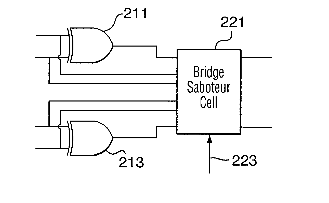
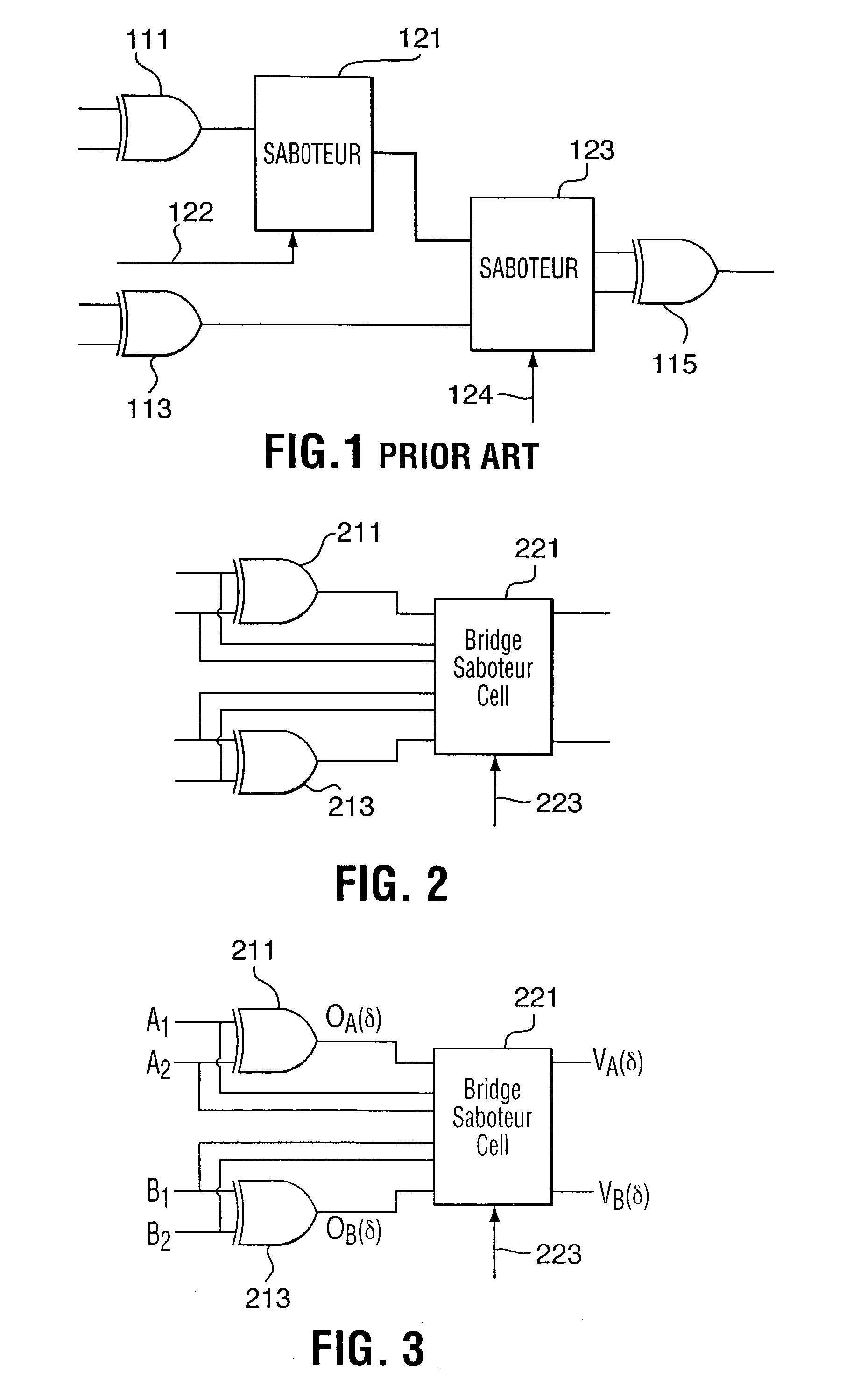
Prior art bridge fault models, which may include saboteurs, are unable to simulate the effects of bridging faults that are input pattern dependent or to determine the drive strength of the signal.
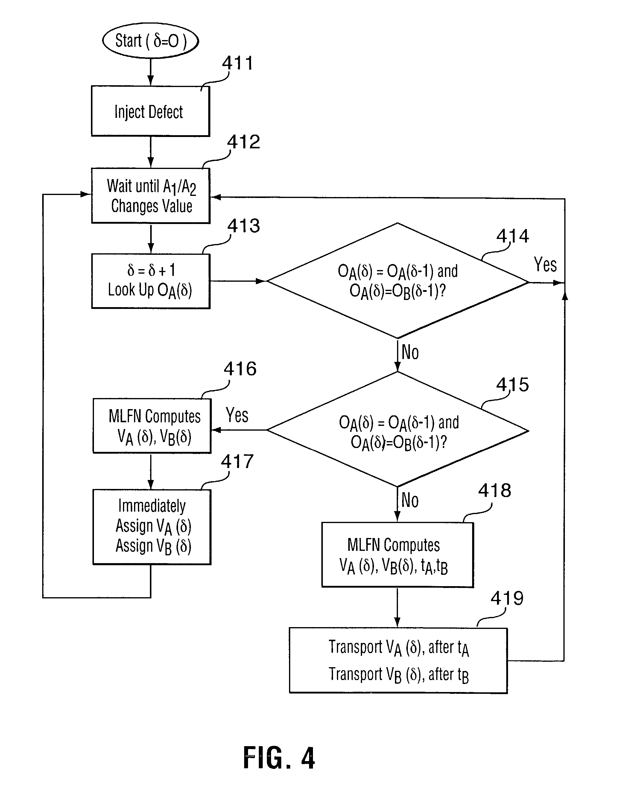
However, the propagation delay computations depend on several additional parameters.
The Byzantine General's problem occurs when the bridged lines adopt an intermediate voltage level, with downstream cells interpreting this voltage at different logic values.
During the training beyond 6000 iterations, the neural network is learning irrelevant details about the training set with respect to the general bridge defect population, which can negatively affect performance for samples not in the training set.
Nonetheless, FIG. 8 indicates that the existing network predicts the node voltages surrounding bridge defects.
Given that moderate sized VHDL structural circuit description typically contains several thousand individual cells, the task of manually inserting bridge faults and analyzing the simulation results is difficult.
However, since close physical proximity between nodes is generally required for bridging defects to occur, the majority of cases in the exhaustive or randomly selected subset are physically difficult.

Method used


Image

  • Method and apparatus for modeling and simulating the effects of bridge defects in integrated circuits
  • Method and apparatus for modeling and simulating the effects of bridge defects in integrated circuits
  • Method and apparatus for modeling and simulating the effects of bridge defects in integrated circuits

Examples


Embodiment Construction

Validation of Bridging Fault Device

[0078] To test the new bridge fault model and defect injection mechanism, a few sample circuits were selected from publicly available sources. Specifically, RTL VHDL descriptions of circuits b11, b14, and b21 were synthesized using the 0.35.mu. cell library described previously. A sample list of characteristics of these benchmark circuits are presented in Table 1 below. For each benchmark circuit, a test pattern file with 200 test vectors was generated pseudorandomly using the bridge fault analysis tool. Then, after the defect-free simulation, bridge defect lists were randomly generated and simulations were conducted for the three circuits as detailed in Table 2 below.

[0079] All simulations were run on a Sun Ultra.TM. Enterprise 4500 server, utilizing 10.times.400 MHz UltraSPARC II.TM. processors. The number of bridge defects reported in the table includes an equal number of soft and hard defects. Each circuit was simulated at two different clock s...


PUM


Abstract

A bridge fault modeling and simulation apparatus including a neural network simulates the effects of bridge defects in complementary metal oxide semiconductor integrated circuits. The apparatus includes a multilayer feedforward neural network (MLFN), implemented within the framework of a very high speed integrated circuit hardware description language (VHDL) saboteur. The saboteur is placed between logic cells in the IC simulation. The apparatus computes exact bridged node voltages and propagation delay times with due attention to surrounding circuit elements. It results in faster simulation and achieves excellent accuracy.

Description

[0001] Benefit and priority is claimed from United States provisional patent application Serial No. 60 / 348,339 filed Oct. 29, 2001, which is currently pending and is hereby incorporated by reference into this application.[0002] The present invention relates to modeling and simulation of bridge defects in integrated circuits with emphasis on complementary metal oxide semiconductor integrated circuits.BACKGROUND INFORMATION[0003] Bridge defects account for most of the defects in complementary metal oxide semiconductor (CMOS) integrated circuits (ICs). Considering that a high percentage of layout area is used by interconnect routing between cells, it has been found that the majority of bridge defects occur between the output signals of logic gates.[0004] A bridge defect between two gate outputs appears dormant as long as the gates are driving the same logic value. However, when the two gates attempt to adopt different logic values, logic contention occurs. Depending on factors such as ...

Claims


Application Information

Patent Timeline
IPC IPC(8): G01R31/317G01R31/3183G06F11/26G06F17/50G06F19/00
CPCG01R31/318328G06F11/261G01R31/318357
Inventor SHAW, DONALDAL-KHALILI, DHAMINROZON, COME
Owner HER MAJESTY THE QUEEN AS REPRESENTED BY THE MINIST OF NAT DEFENCE OF HER MAJESTYS CANADIAN GOVERNMENT
Learn More