Process for making at least one nanotube between two electrically conducting elements and device for implementing such a process

a technology of electrical conductivity and nanotubes, which is applied in the direction of nanoinformatics, crystal growth process, polycrystalline material growth, etc., can solve the problems of incompatibility of proposed method and mass production, complex process type, and still very tedious methods

Inactive Publication Date: 2003-09-18
COMMISSARIAT A LENERGIE ATOMIQUE ET AUX ENERGIES ALTERNATIVES
View PDF8 Cites 7 Cited by
  • Summary
  • Abstract
  • Description
  • Claims
  • Application Information

AI Technical Summary

Problems solved by technology

4898 (2000)" are used particularly for making nanotubes extending perpendicular to a surface on which precipitation is initiated, and not to make a junction of two electrically conducting elements located on a substrate, since this type of process is much more complex to implement.
This method is still very tedious, to the extent that the operation for manufacturing these nanotubes and the operation for connecting these nanotubes with the electrodes, are two steps that must necessarily be made in sequence.
Therefore, the proposed method is completely incompatible with mass production.
Furthermore, the electrical resistance at the nanotube--electrode contact is very high and is not controlled, and can be as high as 10 Mohm.
However, this manufacturing method makes it necessary to cut all nanotubes made in excess of requirements.
Thus, this method is not suitable for mass production either, particularly due to the addition of a final step for cleaning the assembly formed by the nanotube and the electrodes.
As in the previous method, although the connection of the nanotubes to the electrodes is made while the nanotubes are being made, the proposed method is still unable to control the number of nanotubes made between these two electrodes.
Furthermore, the quality of the junction is not fully controlled either, which makes it necessary to keep only nanotubes for which the connection to electrodes was made easily and successfully.

Method used


Image

  • Process for making at least one nanotube between two electrically conducting elements and device for implementing such a process
  • Process for making at least one nanotube between two electrically conducting elements and device for implementing such a process
  • Process for making at least one nanotube between two electrically conducting elements and device for implementing such a process

Examples


Embodiment Construction

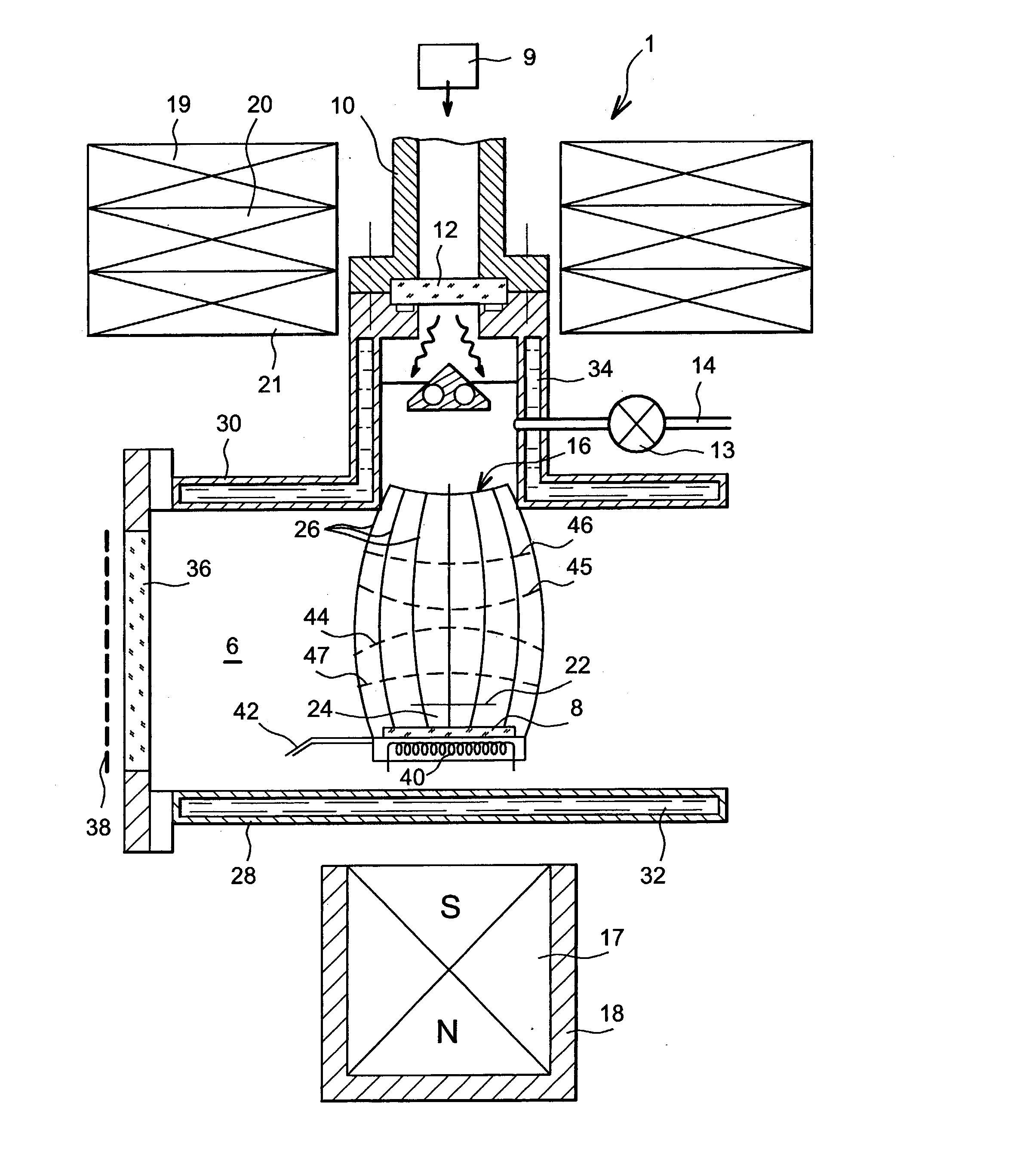
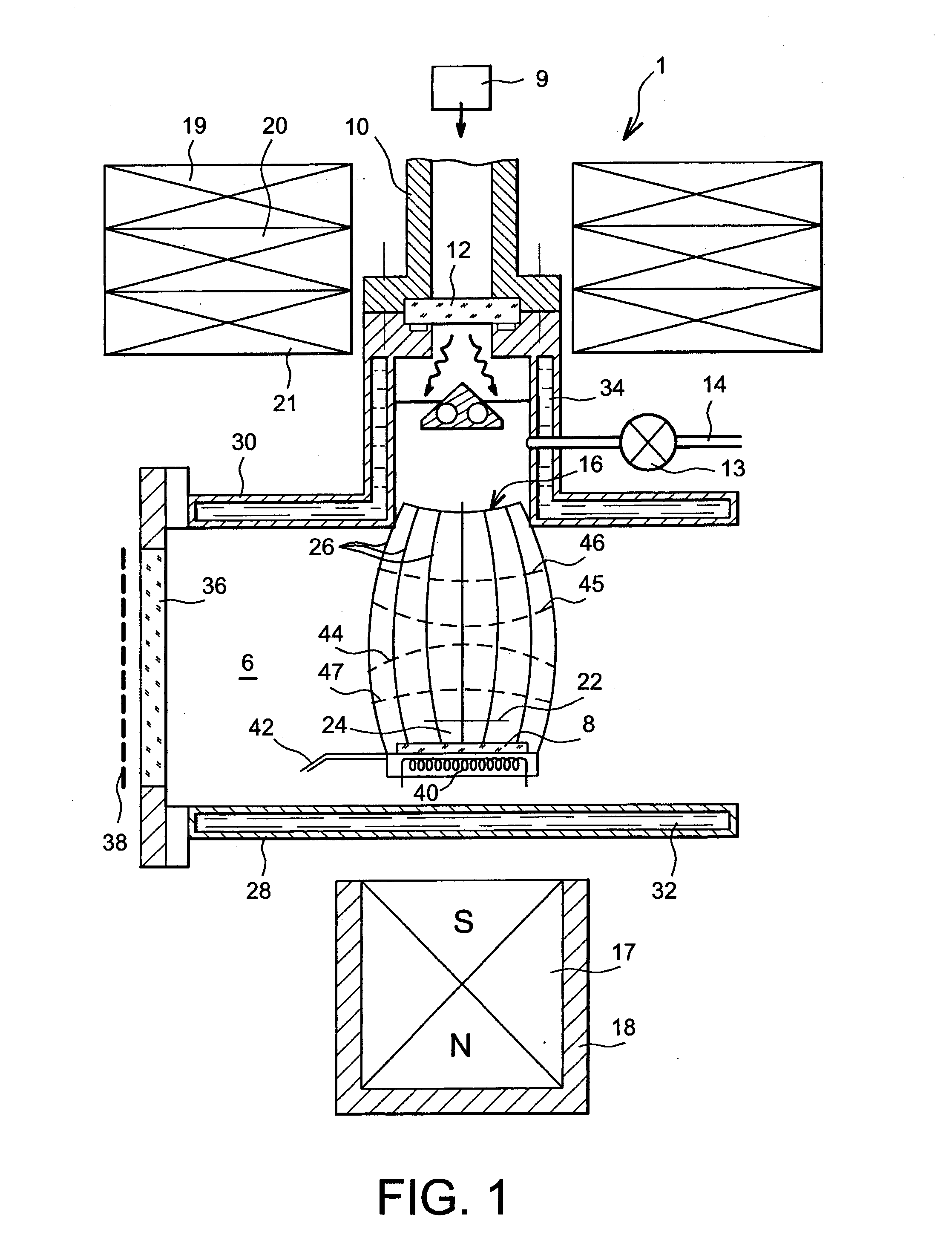
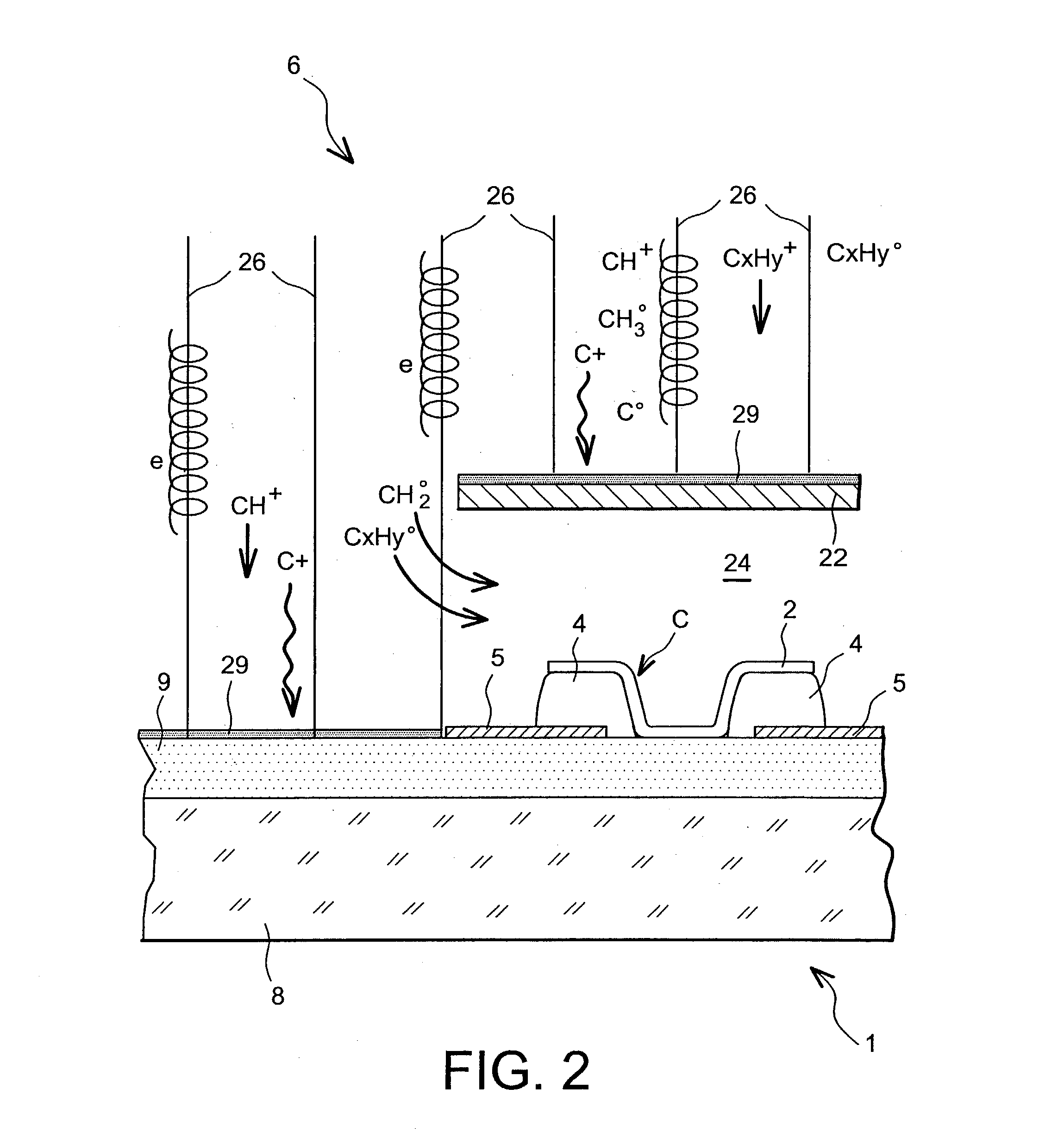
[0049] FIGS. 1 and 2 show a device 1 for making at least one nanotube between two electrically conducting elements 4, by a plasma at electronic cyclotron resonance. These electrically conducting elements 4 are preferably metallic pins comprising a zone containing at least one element such as iron, nickel, cobalt or any other metal or alloy with catalytic fixation and dehydrogenation properties for CxHy.sup.o type non condensable free radicals.

[0050] Note that each electrically conducting element 4 is positioned on an electrical connection electrode 5.

[0051] Still with reference to FIGS. 1 and 2, the device 1 comprises a deposition chamber 6 inside which there is a substrate 8, preferably made of silicon, comprising an insulating layer 9 preferably made of SiO.sub.2. The electrodes 5 and several electrically conducting elements, including the two elements 4 that are to be connected, are supported on this insulating layer 9.

[0052] The deposition chamber 6 is partially delimited by dou...


PUM

PropertyMeasurementUnit
temperatureaaaaaaaaaa
frequencyaaaaaaaaaa

Abstract

This invention relates to a process for making at least one nanotube (2) between two electrically conducting elements (4) located on a substrate (8), the said process using microwave power in a deposition chamber (6), a gas containing organic molecules injected at low pressure inside the deposition chamber (6). According to the invention, the process also uses a magnetic field and at least one electronic cyclotron resonance zone (16) facilitating ionization and/or dissociation of the injected gas, the process also comprising a screening operation of the various species produced in each electronic cyclotron resonance zone (16), in order to exclusively enable CxHyo type non condensable free radicals to access the deposition zone (24) to make the said nanotube. The invention also relates to a device for implementing such a process.

Description

[0001] The technical field of this invention is processes and devices for making nanotubes and / or nanowires (solid nanotubes) comprising carbon atoms, between two electrically conducting elements, the two electrically conducting elements being prelocated on a substrate. "Nanotube" means tubes comprising carbon atoms with a diameter of a few nanometers and a few tens of nanometers, and preferably between 1 and 100 nm.[0002] These assemblies are composed of two electrically conducting elements connected to each other through a nanotube, and are used particularly for making nano components in the field of molecular electronics. For example, these assemblies may have an application in field effect transistors, RAM type memories or any type of electronic junction.[0003] It is quite possible to use this type of assembly to make very high density logical architectures or memories, these assemblies having the advantage that they have a relatively simple design.[0004] The assemblies mentione...

Claims


Application Information

Patent Timeline
Patent Type & Authority Applications(United States)
IPC IPC(8): C01B31/02C23C16/26B81C1/00C23C16/511C30B25/10H01L51/00H01L51/30H05H1/46
CPCB82Y10/00Y10S427/102B82Y40/00C01B31/0226C23C16/26C23C16/511C30B25/105H01J37/32192H01J37/3266H01L51/0048H01L51/0052H05H1/46B82Y30/00Y10S977/843C30B29/02C30B29/605C01B32/16H10K85/221H10K85/615
Inventor DELAUNAY, MARCSENILLOU, ANNESEMERIA, MARIE-NOELLE
Owner COMMISSARIAT A LENERGIE ATOMIQUE ET AUX ENERGIES ALTERNATIVES
Why Eureka
Try Eureka