
Capacitor for analog circuit, and manufacturing method thereof

a technology of capacitors and capacitors, applied in the direction of capacitors, electrical devices, semiconductor devices, etc., can solve the problems of vacancies remaining, the above described techniques for fabricating capacitors are not suitable for manufacturing capacitors, and the dram has required a larger scaled integration and operation voltage, and achieve excellent high voltage resistan

Inactive Publication Date: 2002-10-31
TOKYO ELECTRON LTD
View PDF0 Cites 6 Cited by
  • Summary
  • Abstract
  • Description
  • Claims
  • Application Information

AI Technical Summary

Benefits of technology

[0009] The present invention has been made in consideration of the above, it is an object of the present invention to provide a capacitor having large capacitance and excellent high voltage resistance, and a method for manufacturing the capacitor.
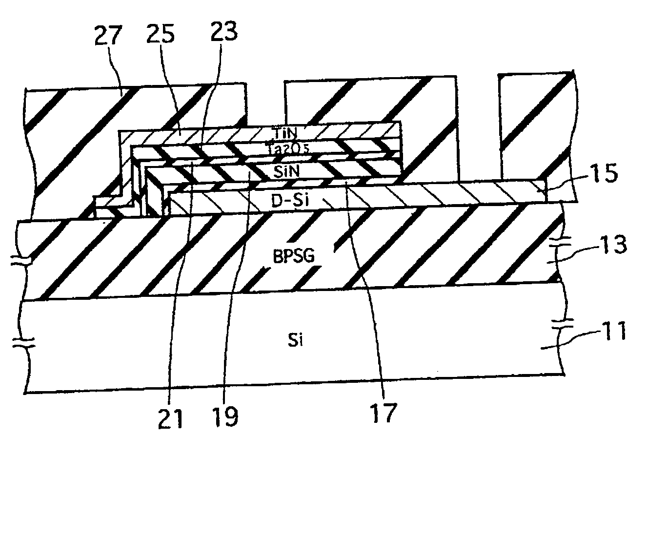
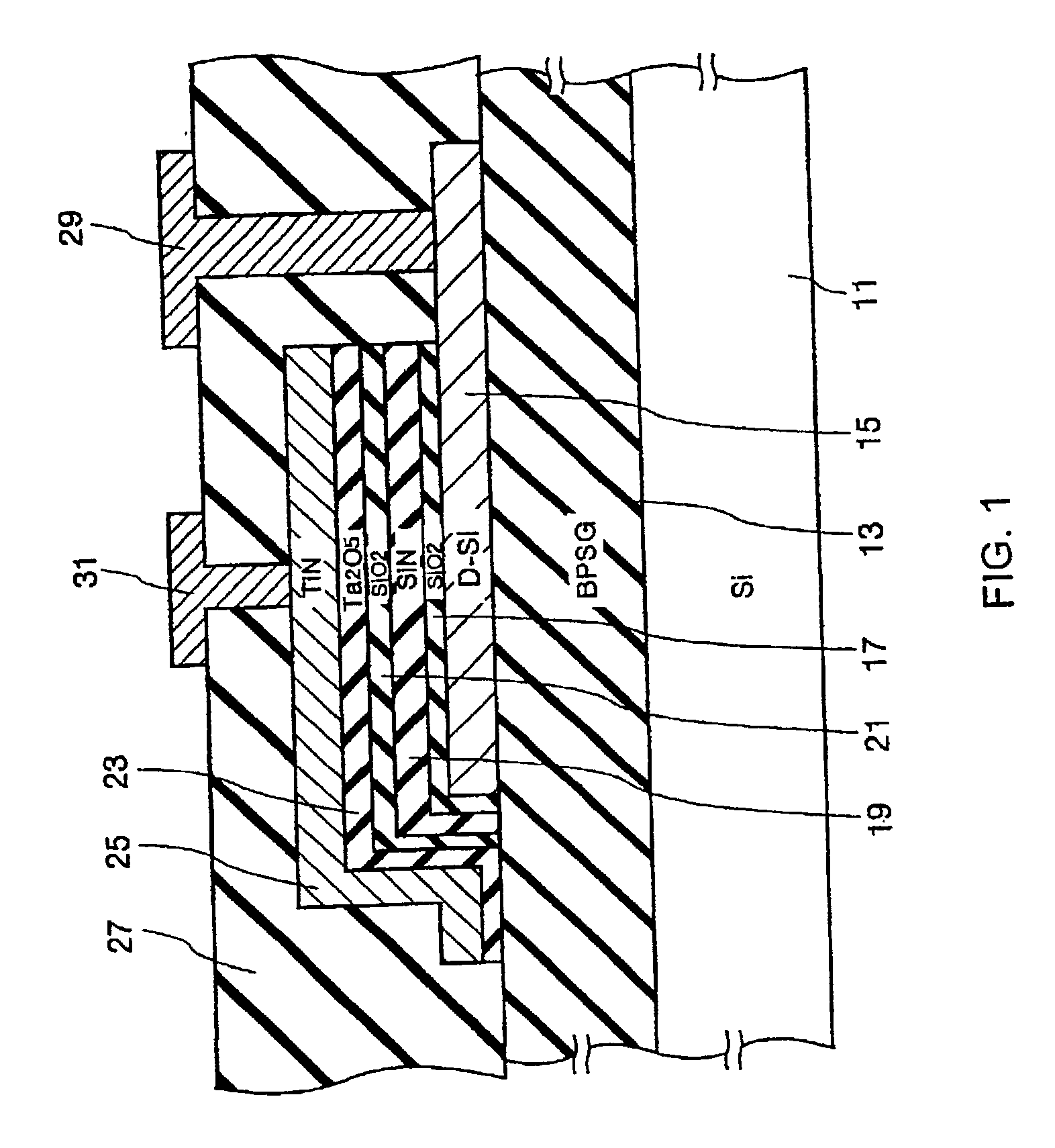
[0035] The nitride film 19 is a silicon nitride film having the thickness of 0.5 to 2.0 nm which is formed by nitridating the lower electrode 15 with, for example, RTN (Rapid Thermal Nitridation) under nitride atmosphere such as nitrogen and ammonium. The nitride film 19 insulates the lower electrode 15 from the upper electrode 25 to prevent chemical reaction caused by direct contact between the lower electrode 15 and the dielectric layer 23, and to restrict impurity diffusion into the lower electrode 15.
[0049] Both the deposition apparatuses 64 and 67 form amorphous metal oxide films such as amorphous tantalum oxide films. The deposition apparatuses 64 and 67 forms film with the thermal CVD technique which employs a mixture gas of a supplied gas after bubbling liquid metal alkoxide, such as pentaethoxy tantalum (Ta(OC.sub.2H.sub.5).sub.5) and an oxide gas such as O.sub.2, to carry out film forming. The dual former structure is helpful to improve throughput.
[0083] Further, since total effective thickness of the oxide film between the lower electrode 15 and the dielectric film 23 is set to equal to or greater than 2 nm, leak current is prevented from flowing, thus, excellent high voltage resistance is available.

Problems solved by technology

That is, DRAM has required larger scaled integration and lower operation voltage.
The above described techniques for fabricating capacitors are not suitable for manufacturing the capacitors having large capacitance and excellent high voltage resistance.
This is caused by oxygen vacancies remaining in the tantalum oxide film even if the tantalum oxide film has been oxidized and crystallized.
Further, the thicker the tantalum oxide film becomes, the easier the vacancies appears.
Therefore, it is difficult to form thick tantalum oxide film without oxygen vacancies in a case of an analog circuit which requires thick tantalum film

Method used


Image

  • Capacitor for analog circuit, and manufacturing method thereof
  • Capacitor for analog circuit, and manufacturing method thereof
  • Capacitor for analog circuit, and manufacturing method thereof

Examples


Embodiment Construction

[0084] An example of the present invention will now be described.

[0085] FIG. 8 is a graph showing high voltage characteristics of a capacitor in which the silicon nitride film 41 is formed in the thickness of 1.5 nm and the tantalum oxide film 43 in the thickness of 30 nm formed on the silicon nitride film 41, and those are subjected to dry oxidization under oxygen atmosphere with no moisture during manufacturing process.

[0086] As shown in FIG. 8, density of an electric current (leak current) between the lower electrode 15 and the upper electrode 25 radically increases when the voltage of approximately +5V or -5V is applied to the upper electrode 25 while the reference voltage is set to a voltage at the lower electrode 15.

[0087] In other words, puncture occurs when equal to or greater than +5V or -5V is applied between the lower electrode 15 and the upper electrode 25, thus the capacitor breaks down. That is, the capacitor is not durable for the analog circuit usage because its high...


PUM

PropertyMeasurementUnit
thicknessaaaaaaaaaa
thicknessaaaaaaaaaa
voltageaaaaaaaaaa

Abstract

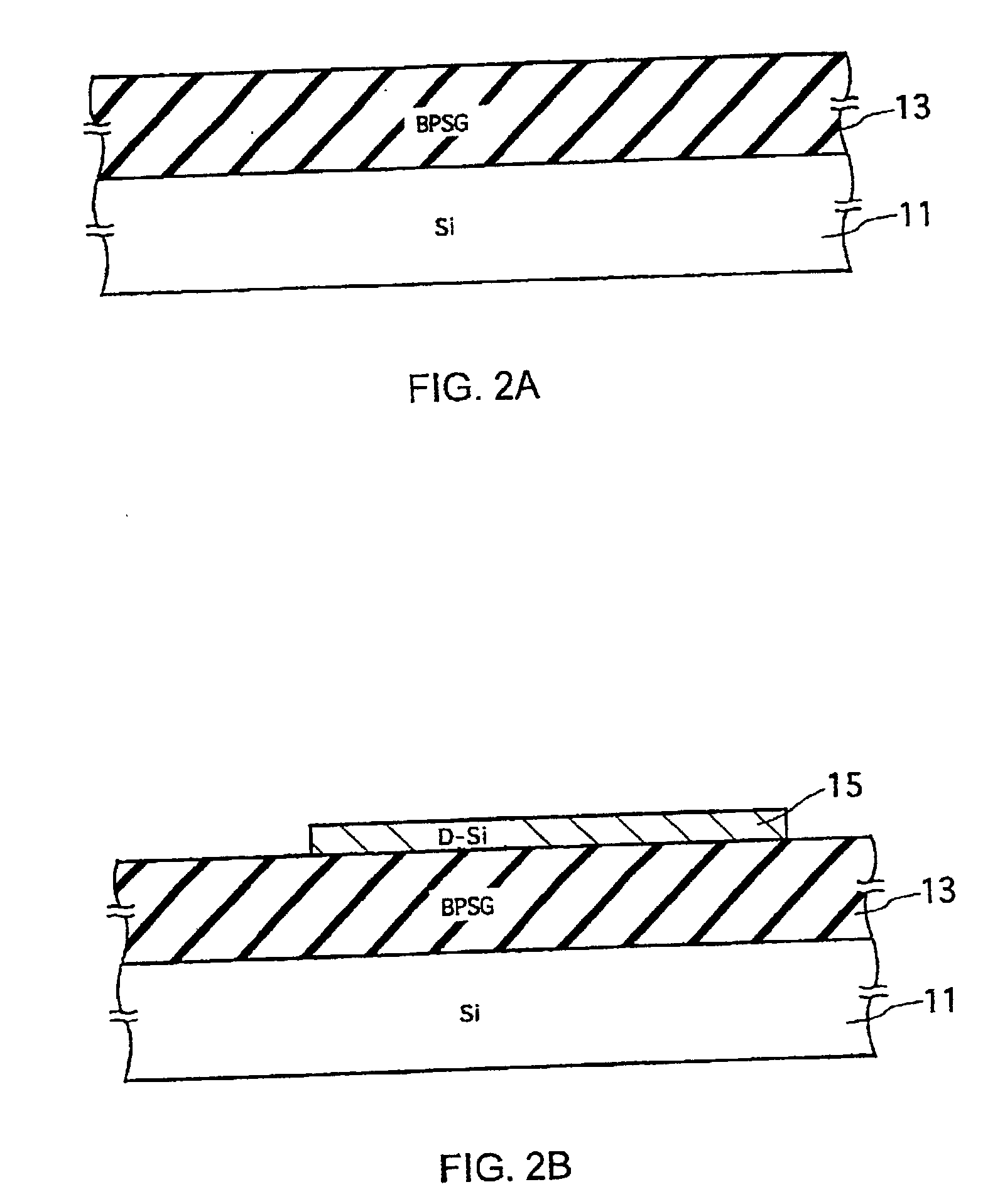
Rapid thermal nitridation is carried out to form a nitride film (19) on a lower electrode (15) which is made of silicon, and a tantalum oxide dielectric film (23) is further formed thereon. Then, wet oxidization is carried out to oxidize the lower electrode through the dielectric film (23) and the nitride film (19), thus an oxide film (17) is formed between the lower electrode (15) and the nitride film (19). Further, silicon which is not bonded to nitrogen in the nitride film (19) is oxidized, thus an oxide film (21) whose effective thickness is equal to or greater than 2 nm. The oxidization also recrystallizes the dielectric film (23). Finally, an upper electrode (25) is formed, and the capacitor is completed.

Description

[0001] The present invention relates to a capacitor applicable to a semiconductor integrated circuit and a manufacturing method of the capacitor. Especially, the capacitor according to the present invention is a capacitor having large capacity and high voltage resistance, thus being suitable for an analog circuit.[0002] One of known capacitors used for a semiconductor device is a capacitor for DRAM (Dynamic Random Access Memory).[0003] Recent design rule to be applied to the DRAM is given in sub micrometers, and required operation voltage has been reduced down to approximately 1.1V. That is, DRAM has required larger scaled integration and lower operation voltage. To overcome those technical difficulties, various structures and manufacturing methods have been proposed.[0004] For example, Unexamined Japanese Patent Application KOKAI Publication No. H9-121035 discloses a method for manufacturing a capacitor. According to the disclosed technique, a capacitor is manufactured as the follo...

Claims


Application Information

Patent Timeline
Patent Type & Authority Applications(United States)
IPC IPC(8): H01L21/02H01L27/04H01L21/314H01L21/316H01L21/321H01L21/822H01L29/94
CPCH01L21/3143H01L21/31604H01L21/32105H01L29/94H01L28/40H01L28/56H01L21/3211H01L21/02183H01L21/02271H01L21/02356H01L21/02345H01L21/02337H01L21/022H01L27/04
Inventor HOSODA, KEIZOMURAKI, YUSUKESATO, ATSUSHIUSHIKAWA, HARUNORI
Owner TOKYO ELECTRON LTD
Learn More