Semiconductor device and manufacturing method thereof

a semiconductor and semiconductor technology, applied in the direction of semiconductor devices, semiconductor/solid-state device details, electrical devices, etc., can solve problems such as serious problems and interconnection problems, and achieve the effect of increasing interconnection resistan

Inactive Publication Date: 2002-09-19
KK TOSHIBA
View PDF0 Cites 5 Cited by
  • Summary
  • Abstract
  • Description
  • Claims
  • Application Information

AI Technical Summary

Benefits of technology

[0007] An object of the present invention is to provide a semiconductor device manufacturing method which enables the formation of highly electromigration-resistant and stress-migration-resistant interconnection divided into fine interconnections shorter than the Blech critical length without increasing the interconnection resistance.
[0009] With the present invention, the inside of the connection holes are filled with the conductive film made of the first substance acting as interconnections thicker than the depth of the connection holes. This prevents the second substance from precipitating in the crystal grain in the conductive film in the connection holes even when the second substance has precipitated at high concentration in the crystal grain in the conductive film outside the connection holes in diffusing the second substance (material for the diffusion barrier layer). On the other hand, the diffusion barrier layer can be formed as far as the bottom of the connection holes, making use of the fact that the diffusion of the second substance in the crystal grain boundary (grain boundary diffusion) is faster than the diffusion in the crystal grain (volume diffusion).
[0010] Specifically, for the conductive film in the connection holes, the second substance is allowed to selectively precipitate in the crystal grain boundary, which prevents the second substance from precipitating in the crystal grain. The precipitation of the second substance in the crystal grain contributes to an increase in the interconnection resistance. Consequently, with the present invention, it is possible to form highly electromigration-resistant fine interconnections without increasing the interconnection resistance.
[0011] On the other hand, stress-migration due to the difference in thermal expansion coefficient between the interconnection and the interlayer insulating film is such a faulty interconnection as a broken interconnection caused by the diffusion of vacancies into a void earlier formed and the accumulation of vacancies in the void. such a faulty interconnection can be prevented by suppressing the long-distance diffusion of voids. In the present invention, the second substance is caused to diffuse into the crystal grain boundary and diffusion barrier layers made of the second substance are allowed to divide the interconnection into fine interconnections. Because the diffusion barrier layers suppress the long-distance diffusion of voids, stress-migration can be prevented. As explained earlier, the formation of such diffusion barrier layers leads to no increase in the interconnection resistance. Therefore with the present invention, the stress-migration resistance of interconnections can be also increased, without increasing the interconnection resistance.
[0012] Another object of the present invention is to provide a semiconductor device capable of increasing the electromigration of interconnection, regardless of the interconnection structure (a damascene structure or an RIE structure).
[0014] The inventors' research has shown that if the above conditions are fulfilled, the electromigration resistance of interconnections can be increased, regardless of the interconnection structure, as described in detail in the embodiments below. Therefore with the present invention, the electromigration resistance of interconnections can be increased, regardless of the interconnection structure. And the diffusion barrier layer also suppress the long-distance diffusion of voids, high stress-migration-resistant can be achieved.

Problems solved by technology

The finer interconnections and multilevel structures have given rise to an interconnection problem.
Since no measure has been taken to reduce the signal current, the current density has been increasing, permitting electromigration (EM) to give rise to broken wires or short circuits, which becomes a serious problem.

Method used


Image

  • Semiconductor device and manufacturing method thereof
  • Semiconductor device and manufacturing method thereof
  • Semiconductor device and manufacturing method thereof

Examples


first embodiment

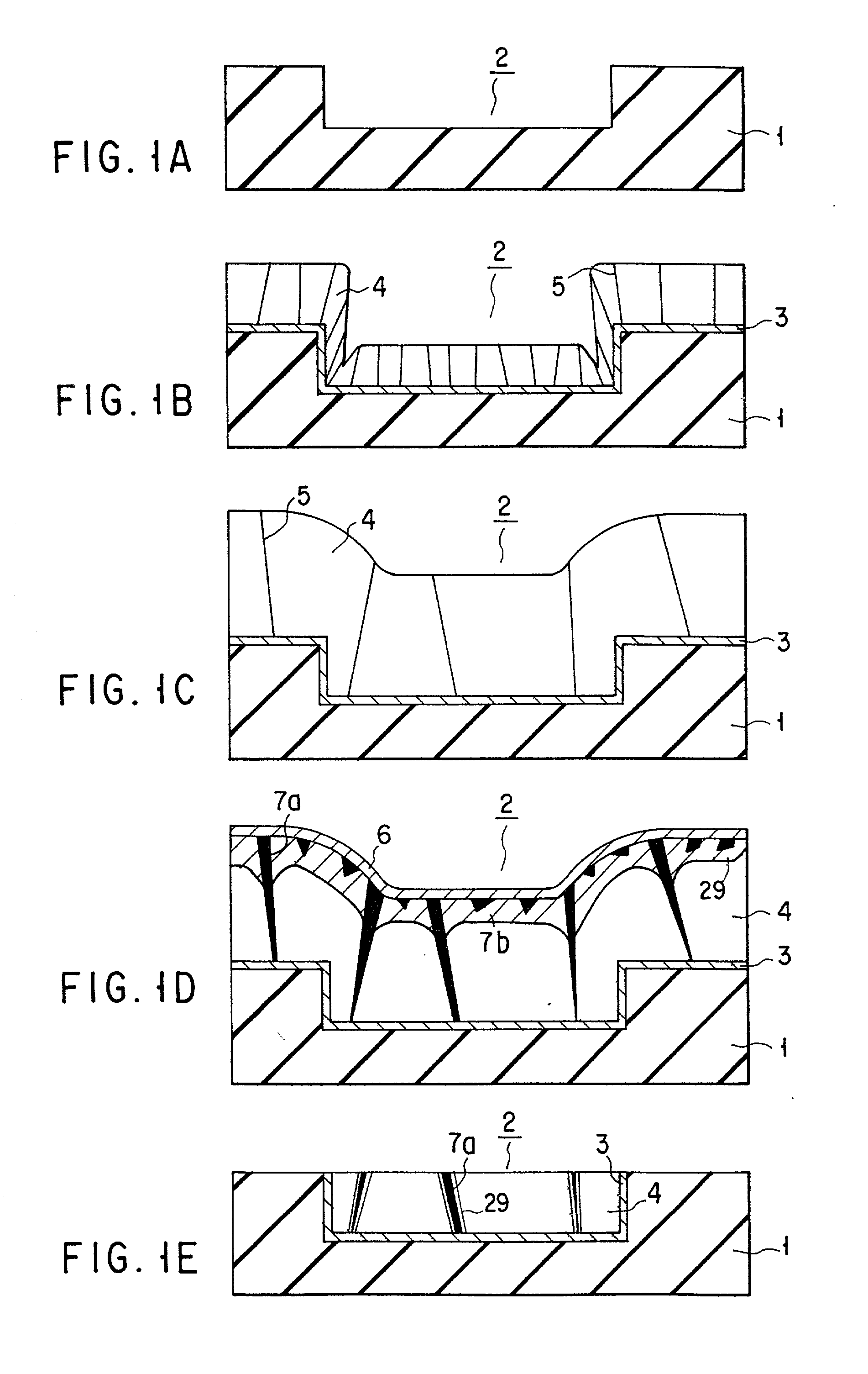
[0030] (First Embodiment)

[0031] Before explanation of embodiments of the present invention, the problems of a conventional equivalent the inventors have found will be described.

[0032] The mentioned forming method has the following problem: the diffusion permits Cu to appear in solid solution and precipitate at high concentration not only in the Al crystal grain boundary but also within the Al crystal grains, resulting in an increase in the resistance of the interconnection.

[0033] The precipitation of Cu in the Al crystal grains takes place as a result of the formation of AlCu compounds in defects at the surface of the Al interconnection caused in embedding the Al interconnection by CMP techniques, which causes the problem of increasing the interconnection resistance.

[0034] The precipitation of Cu in the Al crystal grains prevents a sufficient amount of Cu from precipitating in the Al crystal grain boundary, suppressing the formation of a diffusion barrier layer, which prevents EM re...

second embodiment

[0067] (Second Embodiment)

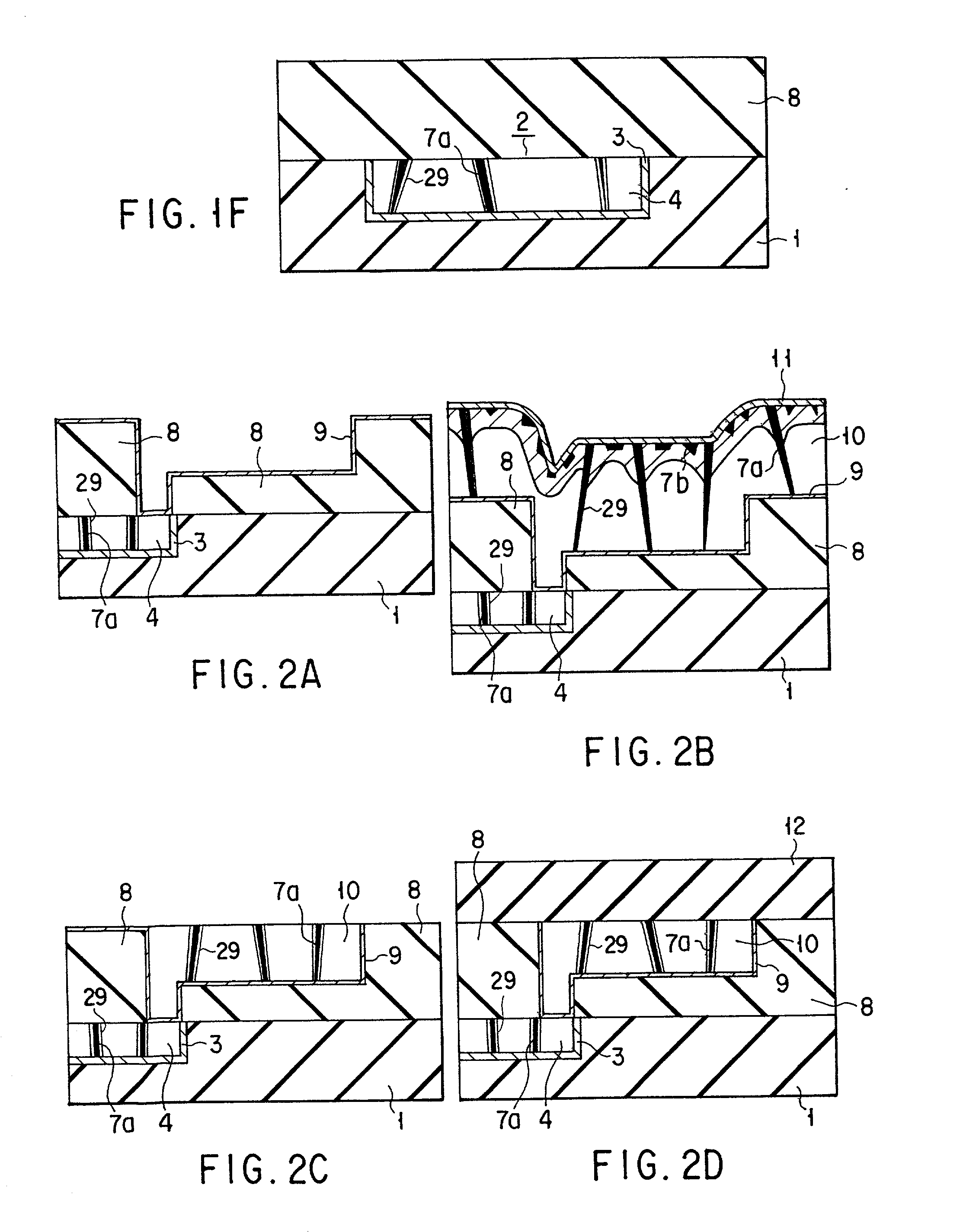
[0068] By the manufacturing method explained in the first embodiment, a semiconductor device having the structure of FIG. 1F is formed. The Cu film forming temperature is changed to 400.degree. C. Next, pads are made in a passivation film 8 by PEP and RIE techniques and thereafter assembling is done. Finally, an aging process is carried out for 15 hours. Namely, at the final process after the assembly, the aging process is performed.

[0069] The inventors formed specimens at various temperature of the aging process (aging temperatures) in the above manufacturing method and measured the interconnection resistance of the Al interconnections for each specimen at room temperature by a four-terminal method. Furthermore, the inventors evaluated the EM resistance of the Al interconnection for each specimen by a conducting test at 225.degree. C. with 2 MA / cm.sup.2. The results are shown in Table 2. The EM test interconnection has both its ends terminated by a W via.

2...

third embodiment

[0075] (Third Embodiment)

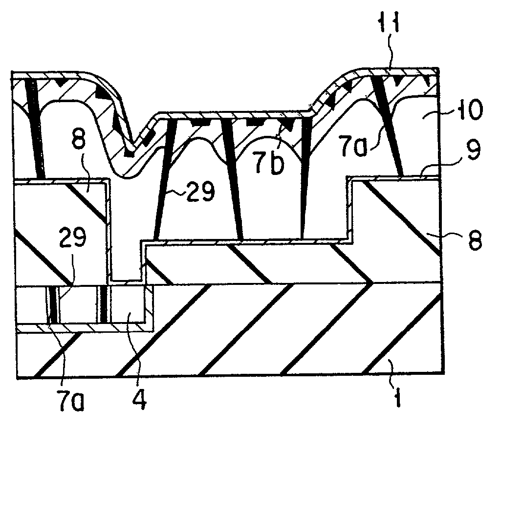
[0076] FIGS. 2A to 2D are sectional views showing a method of manufacturing semiconductor devices according to a third embodiment of the present invention. In FIGS. 2A to 2D, the same parts as those in FIGS. 1A to 1F are indicated by the same reference symbols and a detailed explanation of them will not be given.

[0077] First, the steps of FIGS. 1A to 1E in the first embodiment are carried out. The Cu film forming temperature is set to 400.degree. C. After the substrate temperature has reached about 400.degree. C., the formation of a Cu film 6 is started. The other conditions are the same as those in the first embodiment. As explained in the first embodiment, it is desirable that the Cu film forming temperature should be 150.degree. C. or above but 400.degree. C. or below, preferably 250.degree. C. or above but 350.degree. C. or below.

[0078] Next, as shown in FIG. 2A, a via hole and an interconnection groove connected to the via hole are made in a passivation...


PUM


Abstract

A semiconductor device manufacturing method of the this invention having the step of forming an interlayer insulating film on a semiconductor substrate, the step of making interconnection groove in the interlayer insulating film, the step of filling the inside of the interconnection groove with a conductive film which is made of a first substance and is thicker than the depth of the interconnection groove, the step of thermally stabilizing the size of crystal grains in an Al film either at the same time or after the Al film has been formed, the step of forming a Cu film on the Al film, the step of selectively forming .theta. phase layers in a crystal grain boundary of the Al film by causing Cu to selectively diffuse into the crystal grain boundary of Al film and of allowing the .theta. phase layers to divide the Al film in the interconnection groove into fine Al interconnections shorter than the Blech critical length, and the step of removing the Al film and Cu film outside the interconnection groove.

Description

BACKGROUND OF THE INVENTION[0001] This invention relates to a method of manufacturing semiconductor devices.[0002] As recent semiconductor devices increase in circuit density and performance, interconnections are getting finer and making more use of multilevel structures. Aluminum, Al, has been used as a material for interconnection because it is easy to work and has a relatively low resistance.[0003] The finer interconnections and multilevel structures have given rise to an interconnection problem. Specifically, as interconnections become finer, the cross-sectional area of the interconnection becomes increasingly small. Since no measure has been taken to reduce the signal current, the current density has been increasing, permitting electromigration (EM) to give rise to broken wires or short circuits, which becomes a serious problem.[0004] To solve the problem, a method has been proposed. In the method, diffusion barrier layers against Al are formed in the Al interconnections and th...

Claims


Application Information

Patent Timeline
IPC IPC(8): H01L21/3205H01L21/4763H01L21/768H01L23/48H01L23/52H01L23/532
CPCH01L21/32051H01L21/76814H01L21/76826H01L21/76847H01L21/76867H01L21/76877H01L21/76883H01L23/53223H01L2924/0002H01L2924/00
Inventor HASUNUMA, MASAHIKOKANEKO, HISASHISHIMA, SHOHEIITO, SACHIYO
Owner KK TOSHIBA
Why Eureka
Try Eureka