
Nitride semiconductor growth method, nitride semiconductor substrate, and nitride semiconductor device

a growth method and semiconductor technology, applied in the growth process of crystals, semiconductor lasers, gel state, etc., can solve the problems of not having a practical gan bulk crystal like the one from which many wafers are cut to be used as substrates for the growth of nitride semiconductor layers, not having a lattice-matched nitride semiconductor, and difficult to obtain a nitride semiconductor crystal having good quality

Inactive Publication Date: 2002-04-25
NICHIA CORP
View PDF38 Cites 122 Cited by
  • Summary
  • Abstract
  • Description
  • Claims
  • Application Information

AI Technical Summary

Problems solved by technology

There is, however, no substrate that is lattice-matched with a nitride semiconductor, has excellent crystallinity, and allows a nitride semiconductor crystal-to be stably grown.
That is, any practical GaN bulk crystal like the one from which many wafers are cut to be actually used as substrates for the growth of nitride semiconductor layers has not been obtained.
However, since the ZnO buffer layer grown on the sapphire substrate has poor crystallinity, it is difficult to obtain a nitride semiconductor crystal having good quality by growing a nitride semiconductor on the buffer layer.
In addition, it is difficult to continuously grow a nitride semiconductor thick enough to be used as a substrate on the thin ZnO buffer layer.

Method used


Image

  • Nitride semiconductor growth method, nitride semiconductor substrate, and nitride semiconductor device
  • Nitride semiconductor growth method, nitride semiconductor substrate, and nitride semiconductor device
  • Nitride semiconductor growth method, nitride semiconductor substrate, and nitride semiconductor device

Examples


example 1

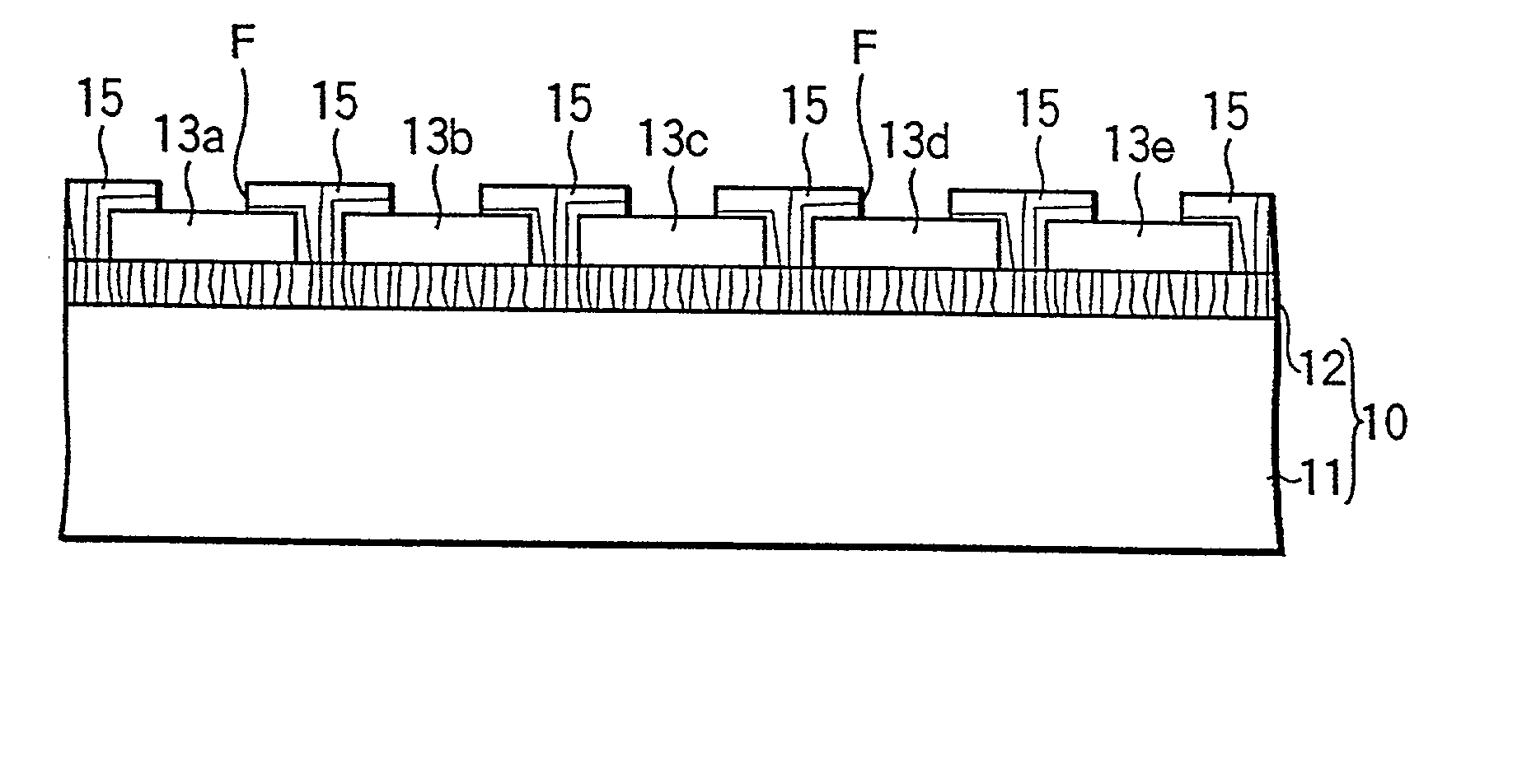
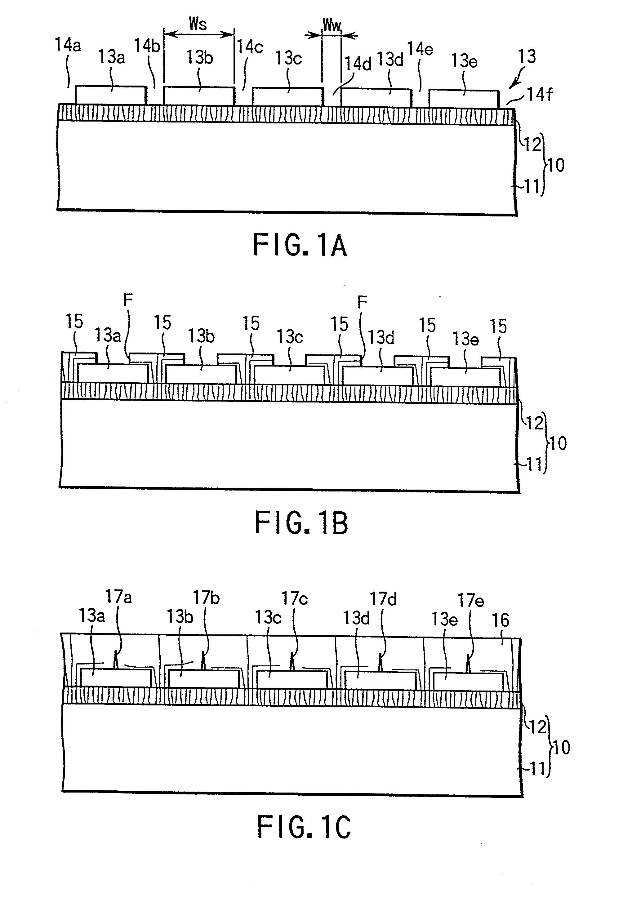
[0138] This example will be described with reference to FIGS. 1A to 1C.

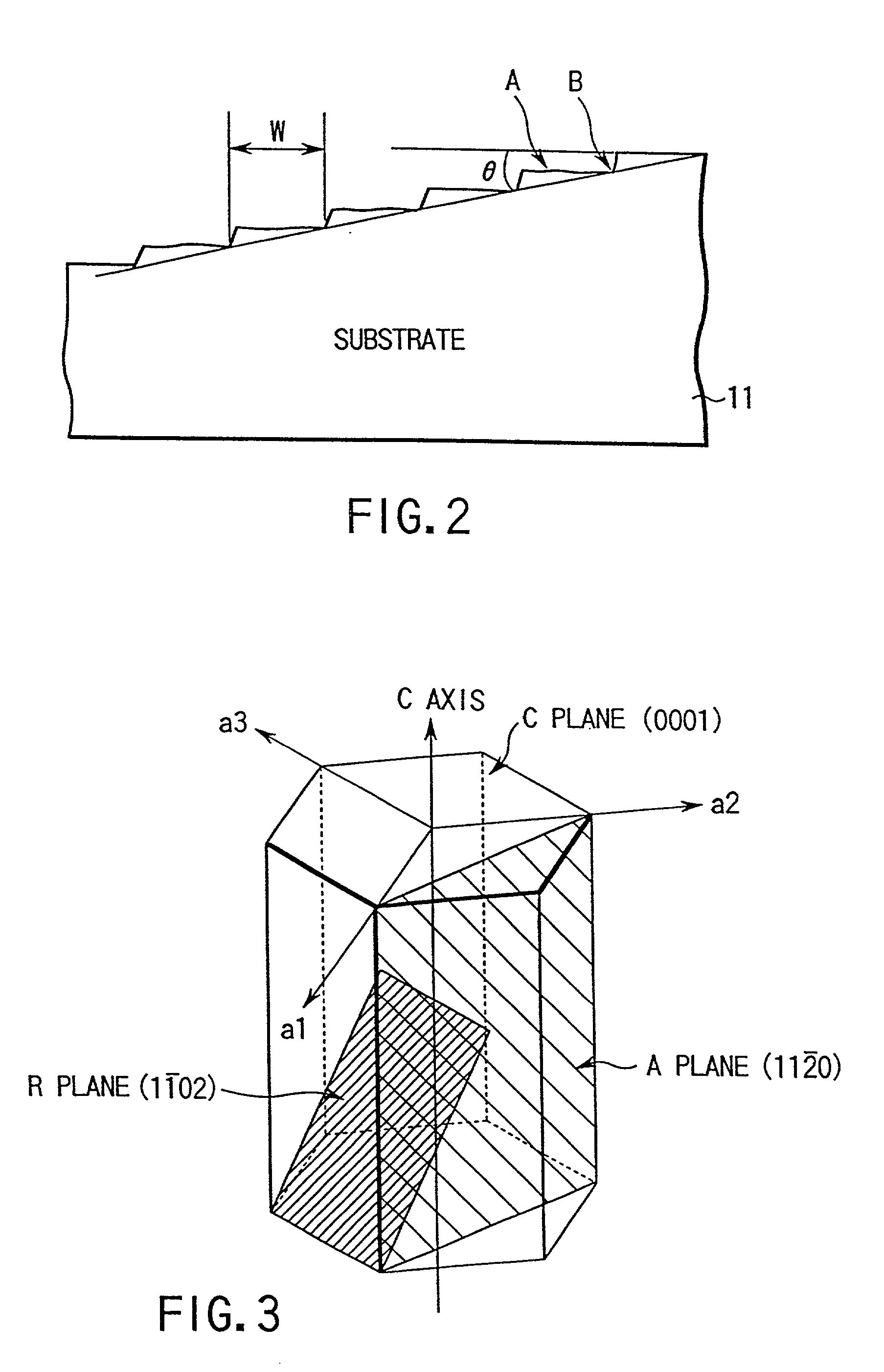
[0139] First of all, a striped photomask was formed on a sapphire substrate 11, 2 inches in diameter, having a C plane as a major surface and an ORF surface forming an A plane, and 0.1-.mu.m thick selective growth masks 13 made of many SiO.sub.2 stripes having a stripe width of 10 .mu.m and a stripe interval (width of each window) of 6 .mu.m were formed by using a CVD apparatus. The respective stripe masks were formed to extend parallel in a direction perpendicular to the ORF surface.

[0140] The sapphire substrate 11, on which the selective growth masks 13 were formed, was set in an MOVPE reaction vessel. A low-temperature buffer layer (not shown) made of GaN was then grown on the substrate 11, on which the selective growth masks 11 were formed, to a thickness of about 200 angstroms at a temperature of 510.degree. C. by using hydrogen as a carrier gas and ammonia and TMG as source gases. This low-temperature buffe...

example 2

[0145] This example will be described with reference to FIGS. 6A to 6C.

[0146] Second selective growth masks 113 having a stripe width of 10 .mu.m and a stripe interval of 6 .mu.m were grown on the surface of a GaN crystal 16 obtained as in Example 1 to a thickness of 0.1 .mu.m in the same manner as in Example 1. The positions of the second selective growth masks 113 were shifted from those of first selective growth masks 13. More specifically, mask alignment was performed such that the respective stripes of the second selective growth masks 113 were located at positions corresponding to windows 14 of the first selective growth masks and extend parallel to the first selective growth masks 13.

[0147] The wafer, on which the second selective growth masks 113 were formed, was placed back into the MOVPE reaction vessel, and a GaN crystal 116 doped with Si at 1.times.10.sup.18 / cm.sup.3 was grown to a thickness of 150 .mu.m by using TMG and ammonia as source gases and silane gas as a dopant...

example 3

[0149] This example will be described with reference to FIGS. 1A to 1C and 6A to 6C.

[0150] A low-temperature buffer layer made of GaN was grown on a sapphire substrate 11 as in Example 1 to a thickness of 200 angstroms, and an undoped GaN layer was grown on the buffer layer to a thickness of 5 .mu.m, thereby forming an underlayer 12 having a two-layer structure. First selective growth masks 13 made up of many SiO.sub.2 stripes having a stripe width of 10 .mu.m and a stripe interval of 8 .mu.m were grown on the flat surface of the underlayer 12 of a support member 10, obtained in this manner, to a thickness of 0.1 .mu.m by the same method as in Example 1. The first selective growth masks 13 extended parallel in a direction perpendicular to the sapphire A plane.

[0151] The wafer, on which the first selective growth masks 13 were formed, was moved into the MOVPE reaction vessel. An undoped GaN crystal 16 was then grown on the wafer to a thickness of 10 .mu.m at 1,050.degree. C. by using...


PUM

PropertyMeasurementUnit
widthaaaaaaaaaa
widthaaaaaaaaaa
widthaaaaaaaaaa

Abstract

A method of growing a nitride semiconductor crystal which has very few crystal defects and can be used as a substrate is disclosed. This invention includes the step of forming a first selective growth mask on a support member including a dissimilar substrate having a major surface and made of a material different from a nitride semiconductor, the first selective growth mask having a plurality of first windows for selectively exposing the upper surface of the support member, and the step of growing nitride semiconductor portions from the upper surface, of the support member, which is exposed from the windows, by using a gaseous Group 3 element source and a gaseous nitrogen source, until the nitride semiconductor portions grown in the adjacent windows combine with each other on the upper surface of the selective growth mask.

Description

[0001] The present invention relates to a nitride semiconductor growth method, a nitride semiconductor substrate, and a nitride semiconductor device and, more particularly, to a method of growing a nitride semiconductor having good crystal quality by using a substrate made of a material different from a nitride semiconductor, a nitride semiconductor substrate, and a nitride semiconductor device.[0002] It is generally known that a semiconductor having few crystal defects and good crystallinity is grown on a substrate by using a substrate lattice-matched with the semiconductor to be grown. There is, however, no substrate that is lattice-matched with a nitride semiconductor, has excellent crystallinity, and allows a nitride semiconductor crystal-to be stably grown. For this reason, there is no choice but to grow a nitride semiconductor on a substrate, e.g., a sapphire, spinnel, or silicon carbide substrate, that is not lattice-matched with nitride semiconductors.[0003] Various research...

Claims


Application Information

Patent Timeline
Patent Type & Authority Applications(United States)
IPC IPC(8): C23C16/04C23C16/30C30B25/02H01L21/20H01L21/205H01L33/00H01L33/16H01S5/02
CPCB82Y20/00H01L21/02639C23C16/303C30B25/02C30B29/40C30B29/403C30B29/406H01L21/0237H01L21/02433H01L21/02458H01L21/02502H01L21/0254H01L21/0262H01L21/02642H01L21/02647H01L33/007H01L33/16H01S5/0213H01S5/0422H01S5/2201H01S5/3202H01S5/3211H01S5/3216H01S5/34333H01S2301/173H01S2304/12H01L21/0242H01L21/02576C23C16/042H01S5/32025
Inventor KIYOKU, HIROYUKINAKAMURA, SHUJIKOZAKI, TOKUYAIWASA, NARUHITOCHOCHO, KAZUYUKI
Owner NICHIA CORP
Learn More