
Large area display and method for making same

a large-area display and display technology, applied in the field of micro-displays, can solve the problems of limiting the size, configuration and function of current hmds, conductive balls of acf may not be sufficiently compressed when connecting, and the anisotropy of conductivity, so as to minimize the burden and cost of sub-block design, and cure the deficiencies

Active Publication Date: 2022-09-06
EMAGIN CORP
View PDF58 Cites 0 Cited by
  • Summary
  • Abstract
  • Description
  • Claims
  • Application Information

AI Technical Summary

Benefits of technology

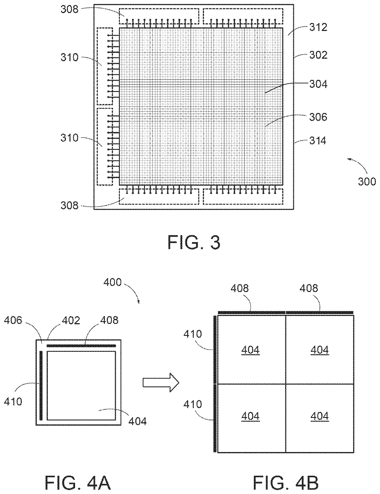
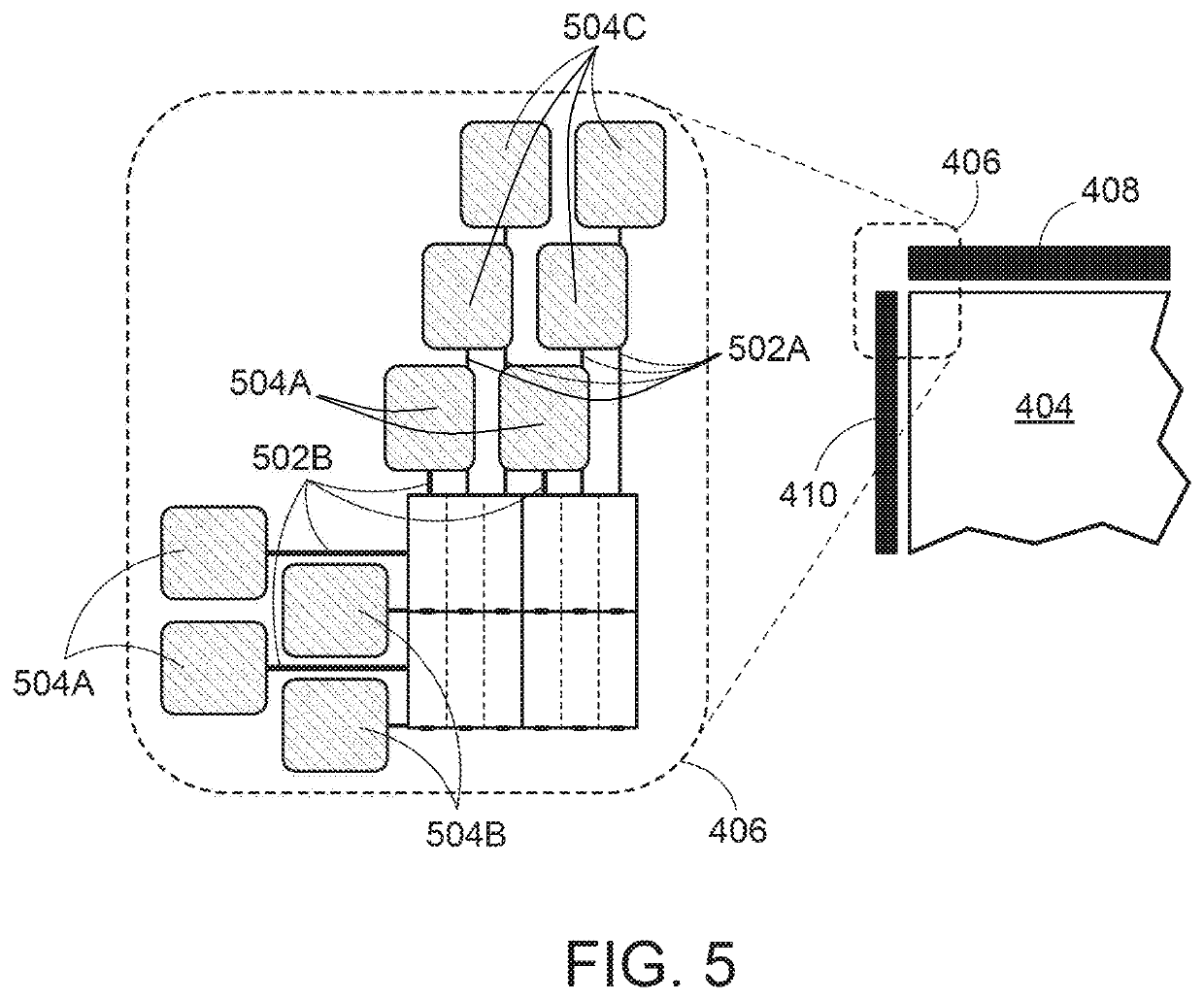
[0016]The present invention cures the deficiencies in the prior art by providing a method to implement a backplane design that is larger than possible with a single exposure of conventional silicon lithography tools while minimizing the burden and cost of the sub-block design.

Problems solved by technology

Such displays place limitations on the size, configuration, and function of current HMDs.
The anisotropy of the conductivity is the result of having the conducting elements in low enough concentration that they only infrequently touch to provide limited lateral conductivity.
Therefore, conductive balls of the ACF may not be sufficiently compressed when connecting, e.g., the FPC and COG to the pads.
Thus, contact failure may occur between the pads and the FPC and COG.
These solutions are limited in the resolution they can achieve to about 600 ppi today with future capability extending to perhaps 1000 ppi.
Technical and production issues will make this very difficult to achieve using TFT on glass for the backplane driver.
For one thing, the low mobility of TFT devices dictates rather large feature sizes to adequately drive an OLED pixel.
Second, the lithography equipment used to pattern the large glass sheets that form the substrates for mobile display panels are limited to resolving feature sizes of greater than 1.5 microns.
However, the size of panels that can be built this way is limited to about 25 mm per side due to the exposure size limitations of modern semiconductor lithography equipment.
As a result the OLED-on-silicon technology that can provide high resolution cannot easily achieve the large display panel sizes (>50 mm per side) that are optimal for VR headsets.

Method used


Image

  • Large area display and method for making same
  • Large area display and method for making same
  • Large area display and method for making same

Examples


Embodiment Construction

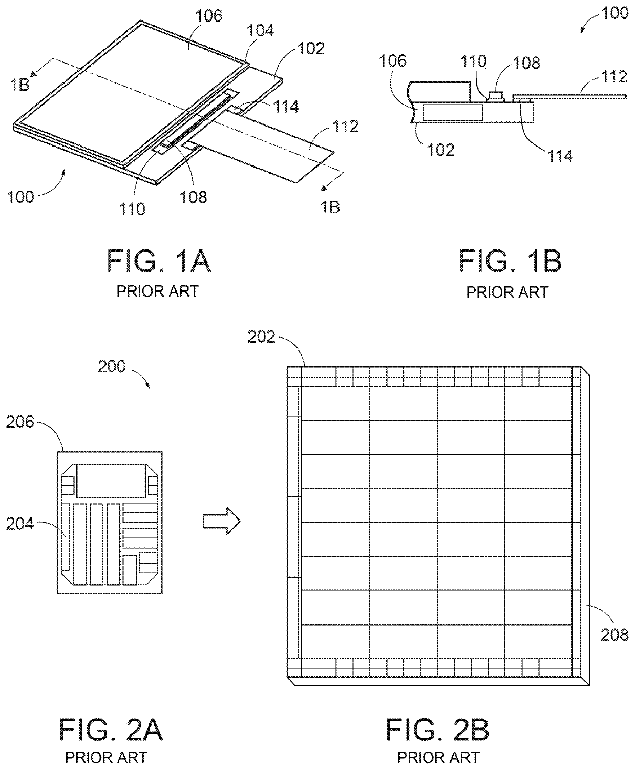
[0030]FIGS. 1A and 1B illustrates a conventional mobile display panel 100 used in virtual reality applications. The panel 100 consists of a polysilicon thin-film-transistor (TFT) 104 on glass backplane 102, with an OLED layer 106 deposited on top. Preferably, the OLED layer 106 is a side-by-side color architecture with each color stack evaporated through a fine metal mask. Separate driver integrated circuits (ICs) 108 are attached to the glass substrate using an anisotropic adhesive film (ACF) layer 110. Separate flexible printed circuits (FPCs) 112 are attached to the glass substrate using an anisotropic adhesive film (ACF) layer 114.

[0031]FIGS. 2A and 2B illustrates a conventional silicon stitching method 200 used to build semiconductor chips 202 at a foundry that are larger than possible with existing patterning tools. The chip 202 is partitioned into sub-blocks 204, which must fit into a single reticle 206. Each sub-block 204 is patterned across the wafer 208 in sequence. Method...


PUM

PropertyMeasurementUnit
feature sizesaaaaaaaaaa
sizeaaaaaaaaaa

Abstract

A large area active-matrix organic light-emitting diode microdisplay and method for fabricating the same is provided which includes a panel having resolution of greater than 2,000 pixels per inch and a size of 1.4 or more inches for supporting the needs of virtual reality and augmented reality application.

Description

STATEMENT OF RELATED CASES[0001]This case claims priority to U.S. Provisional Patent Application Ser. No. 62 / 398,329 filed on Sep. 22, 2016, which is incorporated herein by reference in its entirety.FIELD OF THE INVENTION[0002]The present invention relates to microdisplays in general, and, more particularly, to a method for making an active-matrix organic light-emitting diode (AMOLED) microdisplay that provides super-resolution and is larger than possible using conventional production methods.BACKGROUND OF THE INVENTION[0003]Immersive head mounted displays (HMDs) in which a virtual reality (VR) or an augmented reality (AR) is displayed to a user include applications in outdoor activities (e.g., hunting, fishing, bird watching), combat training, and video gaming, among others. Conventional immersive HMDs incorporate relatively large (e.g., 4 inches×2 inches), low-resolution displays similar to those found in smartphones, as well as off-the-shelf commercial lenses. Such displays place...

Claims


Application Information

Patent Timeline
Patent Type & Authority Patents(United States)
IPC IPC(8): H01L27/32H01L51/00H01L23/00H01L27/06
CPCH01L27/3255H01L24/83H01L27/326H01L27/3276H01L51/0096H01L27/0629H01L2224/83851H01L2227/323H01L2251/5353H01L2924/1426Y02E10/549H01L2224/16225H10K59/129H10K59/121H10K59/131H10K77/10H10K2102/321H01L2924/00014H10K59/1201
Inventor WACYK, IHORGHOSH, AMALKUMAR P.SCULLEY, JR., ANDREW G.PRACHE, OLIVIER
Owner EMAGIN CORP
Learn More