Thin-layer capacitor and method of fabricating the same
a technology of thin-layer capacitors and capacitors, which is applied in the direction of fixed capacitors, stacked capacitors, fixed capacitor details, etc., can solve the problems of reducing the whole area of the semiconductor device, and the effective use of the area occupied by the mim capacitor in the semiconductor device is a major challeng
- Summary
- Abstract
- Description
- Claims
- Application Information
AI Technical Summary
Benefits of technology
Problems solved by technology
Method used
Image

Examples
embodiment 1
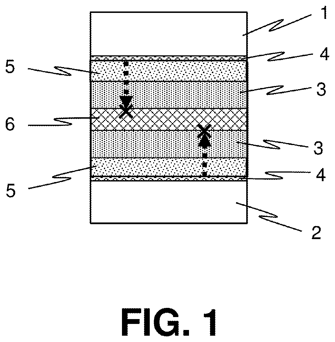
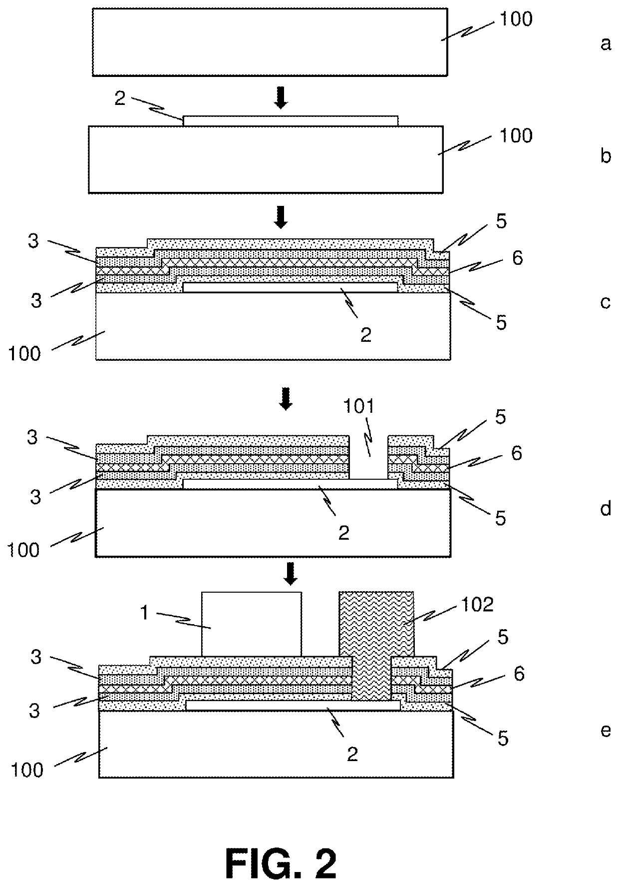
[0028]A cross-sectional view of a thin layer capacitor according to Embodiment 1 of the present application is shown in FIG. 1. The thin layer capacitor is an example of an MIM capacitor formed of a dielectric layer between an upper electrode 1 and a lower electrode 2. To be more specific, the thin layer capacitor is formed such that high-dielectric-constant amorphous insulating films are in contact with the upper electrode 1 and the lower electrode 2, respectively. This is due to the fact that if a high-breakdown-voltage amorphous film 3 is in direct contact with the upper electrode 1 or the lower electrode 2, a defect occurs due to an electric field concentration at the interface 4 between the dielectric layer and the electrode surface having microscopic asperities (referred to also as surface roughness) and a fracture is thereby likely to extend into the high-breakdown-voltage amorphous film 3. Hence, a fracture is prevented by forming the high-dielectric-constant amorphous insul...
embodiment 2
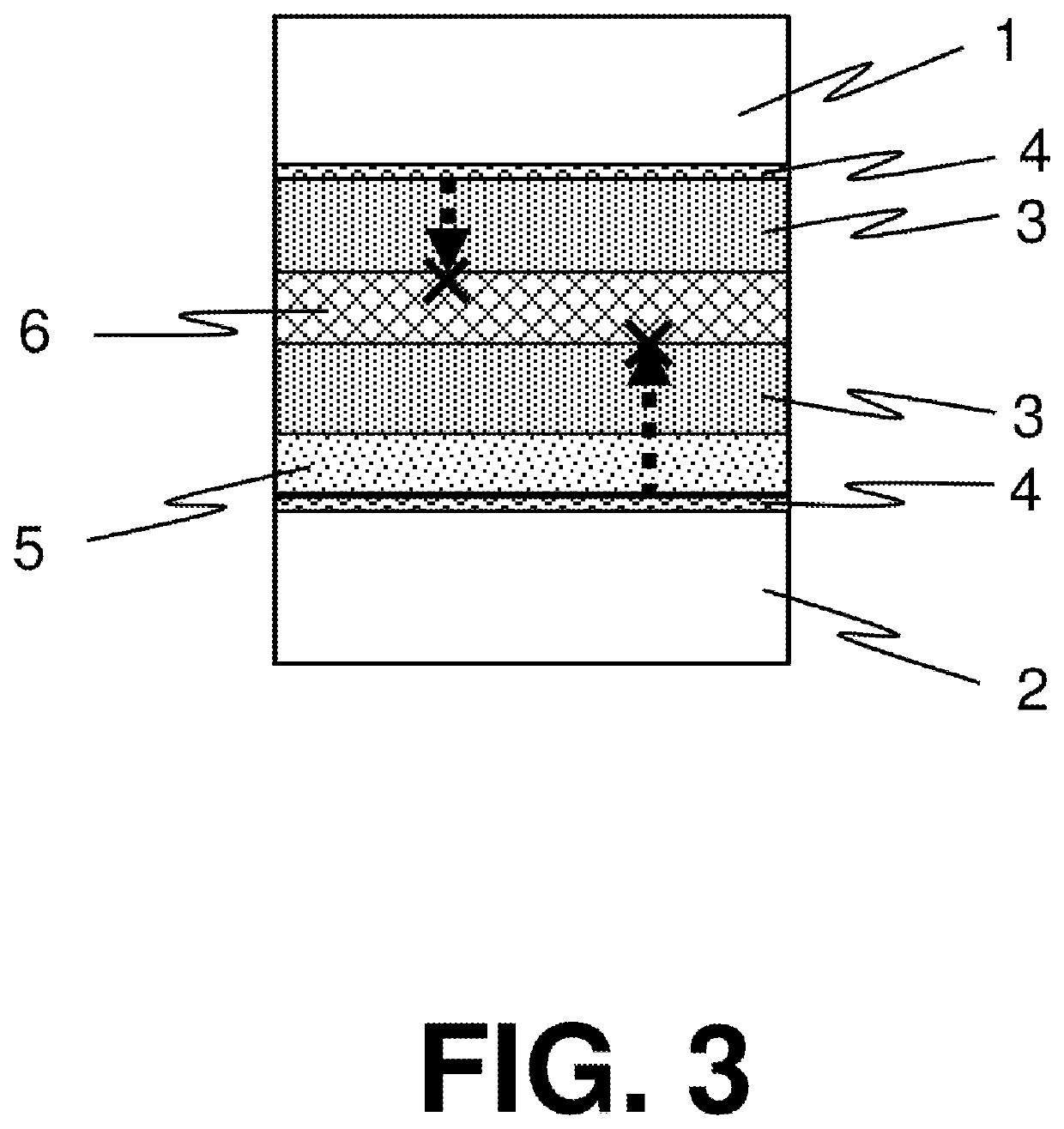
[0038]A cross-sectional view of a thin layer capacitor according to Embodiment 2 of the present application is shown in FIG. 3. The thin layer capacitor of Embodiment 2 is an MIM capacitor that has a configuration such that the high-dielectric-constant amorphous buffer film 5 is in contact only with the lower electrode 2 at the interface 4, i.e., the boundary between the surface of the electrode and the dielectric layer. The configuration other than that is the same as that described in Embodiment 1.
[0039]The thin layer capacitor according to Embodiment 2, although cannot prevent a defect from occurring at the interface between the upper electrode 1 and the high-breakdown-voltage amorphous film 3, has a merit of reducing the number of dielectric films. Note that while the above describes that the configuration of the thin layer capacitor is such that the high-dielectric-constant amorphous buffer film 5 is in contact with only the lower electrode 2, the configuration is not limited t...
embodiment 3
[0040]A cross-sectional view of a thin layer capacitor according to Embodiment 3 of the present application is shown in FIG. 4. In Embodiment 3, a semiconductor 7 is formed instead of the lower electrode 2 of Embodiment 1. In other words, the thin layer capacitor of the present embodiment has a configuration of a metal insulator semiconductor (MIS) capacitor. The configuration other than this is the same as that of the thin layer capacitor of Embodiment 1. Employing this configuration also allows for obtaining the same fracture preventing effect as that of Embodiment 1. Moreover, employing the configuration brings a new effect of being able to apply also to a gate structure of an MIS transistor; hence, an MIC transistor of high reliability can be fabricated.
PUM
| Property | Measurement | Unit |
|---|---|---|
| thickness | aaaaa | aaaaa |
| thickness | aaaaa | aaaaa |
| dielectric constant | aaaaa | aaaaa |
Abstract
Description
Claims
Application Information
 - R&D
- Intellectual Property
- Life Sciences
- Materials
- Tech Scout
- Unparalleled Data Quality
- Higher Quality Content
- 60% Fewer Hallucinations
Browse by: Latest US Patents, China's latest patents, Technical Efficacy Thesaurus, Application Domain, Technology Topic, Popular Technical Reports.
© 2025 PatSnap. All rights reserved.Legal|Privacy policy|Modern Slavery Act Transparency Statement|Sitemap|About US| Contact US: help@patsnap.com