
Coating composition, method for producing organic electroluminescent device using same, and organic electroluminescent device produced thereby

a technology of organic light-emitting diodes and coating compositions, which is applied in the direction of polyether coatings, coatings, solid-state devices, etc., can solve the problems of high equipment investment costs and process costs, high waste of materials, and high percentage of waste without being deposited on the substrate, so as to improve the effect of coating, easy removal, and smooth conversion

Active Publication Date: 2021-08-03
LG CHEM LTD
View PDF27 Cites 0 Cited by
  • Summary
  • Abstract
  • Description
  • Claims
  • Application Information

AI Technical Summary

Benefits of technology

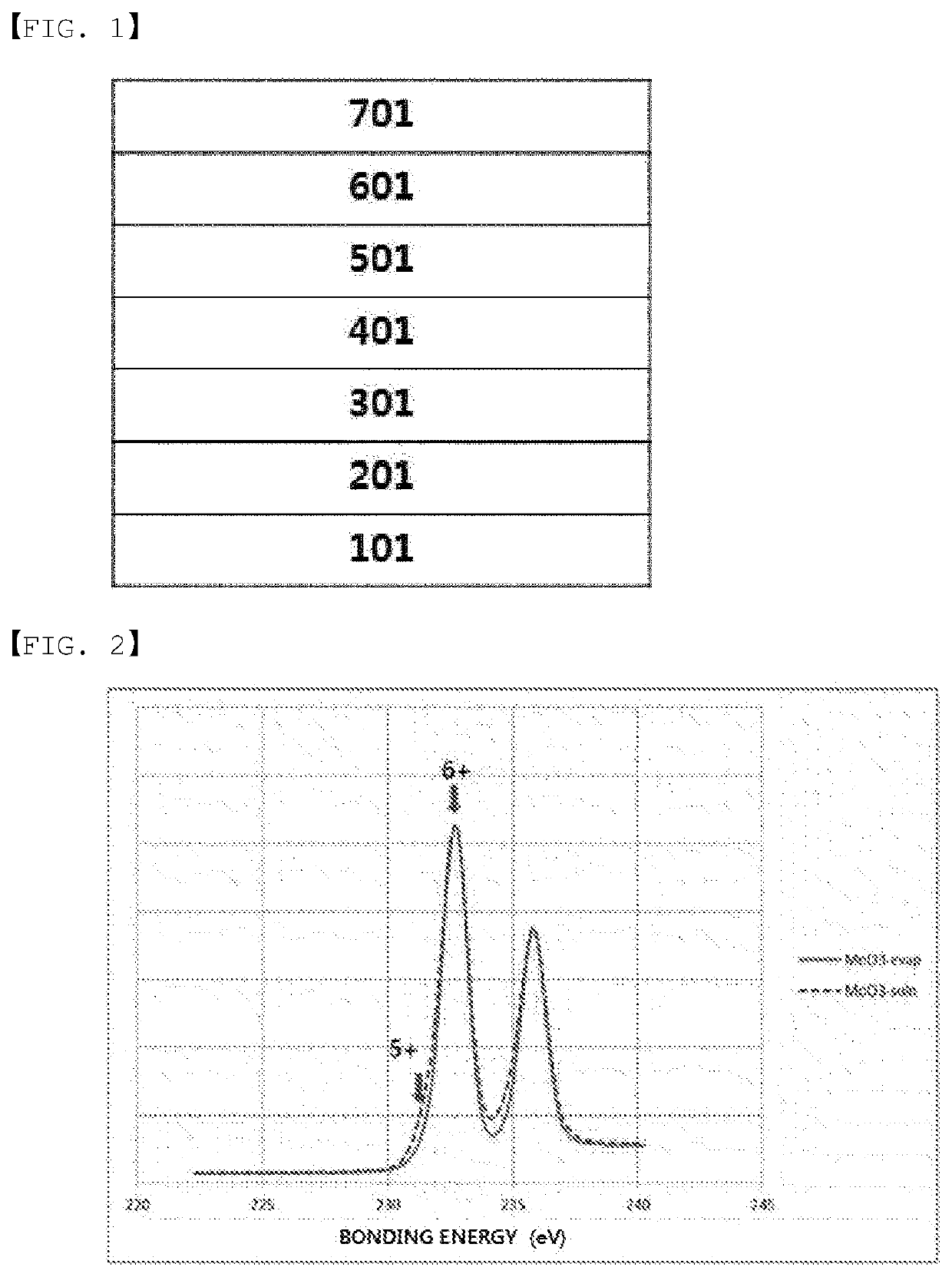
The present patent describes the use of an organic polymer with sulfonic acid and a fluorine group together with an organic metal complex of a transition metal to form a hole injection or transfer layer of an organic light emitting diode. The sulfonic acid acts as an oxidizer, readily removing the organic material ligand of the organic metal complex and converting it to a metal oxide. The organic polymer improves coatability and stability of the hole injection or transfer layer, resulting in a long lifetime of the device. The transition metal oxide, such as MoO3, maintains a high work function with the organic polymer, ensuring smooth hole injection and a long lifetime of the device without voltage increase and efficiency decrease.

Problems solved by technology

When manufacturing an organic light emitting diode using a vacuum process, there are disadvantages in that a burden for high equipment investment costs and process costs is very high, uniformly enlarging the device has limits, and utilization of materials is low since, during deposition, the percentage of being wasted without being deposited on a substrate is high.
However, when laminating layers forming an organic light emitting diode through a solution process, lower layers are likely to be damaged by processes of forming upper layers, unlike in the deposition process.
In other words, materials of lower layers are dissolved again by solvents or inks used in the solution process causing a phenomenon of mixing with upper layers or physically damaging a thin film.
In addition, when using these, a relatively low operating voltage is obtained.
However, these normally use acidic dopant materials with a low pH and damage electrode materials that are lower layers, and thereby have a disadvantage of declining a life time property.
However, as described above, this method still has a problem of post process tolerance for solvents or inks.

Method used


Image

  • Coating composition, method for producing organic electroluminescent device using same, and organic electroluminescent device produced thereby
  • Coating composition, method for producing organic electroluminescent device using same, and organic electroluminescent device produced thereby
  • Coating composition, method for producing organic electroluminescent device using same, and organic electroluminescent device produced thereby

Examples


example 1

[0115]After washing an ITO-coated glass substrate consecutively with water and isopropanol, a solution obtained by mixing MO2(acac)2 and Nafion (following structural formula A) in a ratio of 9:1 and dissolving the result in ethylene glycol monomethyl ether was spin coated on the ITO-deposited base for seconds at 3000 rpm. The obtained thin film was heat treated for 15 minutes at 200° C. under oxygen atmosphere to form a very uniform hole injection layer having a thickness of 30 nm.

[0116]On the top of the hole injection layer, a hole transfer layer having a thickness of 400 Å was formed using a spin coating method by dissolving a hole transfer material represented by the following Chemical Formula B in toluene.

[0117]On the hole transfer layer, a light emitting layer having a thickness of 300 Å was formed by doping BD, a blue dopant, to BH, a blue fluorescent host, in a weight ratio of 95:5.

[0118]Subsequently, on the top of the light emitting layer, an electron transfer layer and an e...

example 2

[0121]A device was manufactured in the same manner as in Example 1 except that the thin film was treated under nitrogen atmosphere.

example 3

[0122]A device was manufactured in the same manner as in Example 1 except that EW825 of 3M (following Chemical Formula D) was used instead of Nafion.

[0123]


PUM

PropertyMeasurementUnit
thicknessaaaaaaaaaa
temperatureaaaaaaaaaa
boiling pointaaaaaaaaaa

Abstract

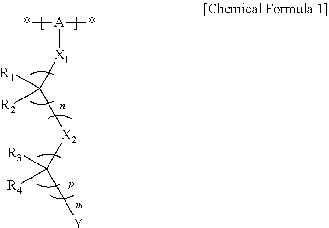
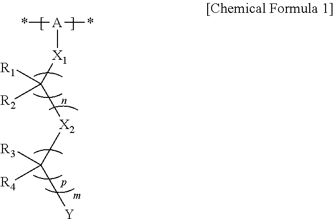
The present specification relates to a hole injection or transfer layer coating composition of an organic light emitting diode comprising an organic metal complex of a transition metal; a fluorine-based polymer comprising sulfonic acid or sulfonate; and an organic solvent, a method for manufacturing an organic light emitting diode and an organic light emitting diode using the same.

Description

CROSS-REFERENCE TO RELATED APPLICATIONS[0001]The present application is a national phase entry under 35 U.S.C. § 371 of International Application No. PCT / KR2017 / 012520 filed Nov. 7, 2017, which claims priority from Korean Patent Application No. 10-2016-0147558 filed Nov. 7, 2016, all of which are incorporated herein by reference.TECHNICAL FIELD[0002]The present specification relates to a coating composition, a method for manufacturing an organic light emitting diode and an organic light emitting diode manufactured using the same.BACKGROUND ART[0003]An organic light emission phenomenon is one of examples converting current to visible light by an internal process of specific organic molecules. A principle of an organic light emission phenomenon is as follows. When an organic material layer is placed between an anode and a cathode and a current is applied between the two electrodes, electrons and holes are injected to the organic material layer from the cathode and the anode, respectiv...

Claims


Application Information

Patent Timeline
Patent Type & Authority Patents(United States)
IPC IPC(8): H01L51/50H01L51/00C09D129/10C09D171/00H10K99/00
CPCH01L51/004C09D129/10C09D171/00H01L51/0035H01L51/0043H01L51/0003H01L51/0005H01L51/5056H01L51/5088C08F16/30C08F28/02C09D141/00H01L21/324H10K85/141H10K85/341H10K50/155H10K50/17H10K71/40H10K50/15H10K85/111H10K85/151H10K71/12H10K71/135
Inventor YOON, SEOKHEELEE, JAECHOLKIM, JINSECKLEE, DONGGUKIM, HWAKYUNGJEONG, JAE HAKSHIN, JIYEONKIM, DAEHO
Owner LG CHEM LTD
Learn More