Current sensor having microwave chip resistors in parallel radial arrangement

a current sensor and resistor technology, applied in the field of current sensor with microwave chip resistors, can solve the problems of reducing the dielectric constant of materials, unable to develop practical specifications for individual components of conventional cdm testers, and difficulty in identifying individual component responses in time domain. to achieve the effect of increasing the resistance of the resistor

Active Publication Date: 2019-04-23
BARTH JON E +1
View PDF5 Cites 1 Cited by
  • Summary
  • Abstract
  • Description
  • Claims
  • Application Information

AI Technical Summary

Benefits of technology

[0015]In certain embodiments in accordance with this aspect, the plurality of chip resistors comprises ten chip resistors. Each resistor has a nominal resistance of approximately 10 ohms. The plurality of ten chip resistors provides a parallel resistance of approximately 1 ohm. In certain embodiments, each of the ten chip resistors comprises a trimmable thin film resistor having a nominal resistance of approximately 10 ohms. Each resistor is selectively trimmable to increase the resistance of the resistor to thereby adjust the parallel resistance to a value closer to 1 ohm.

Problems solved by technology

Identifying the individual component responses in the time domain using conventional CDM testers has proven to be difficult.
Accordingly, no practical specifications have been developed for individual components of the conventional CDM testers.
Supply issues later forced the use of a ring of up to six 6-ohm chip resistors mounted on an FR4 laminate (a glass-reinforced epoxy composite material).
An FR4 laminate has many beneficial physical properties; however, its electrical characteristics may become inconsistent at higher frequencies, where the dielectric constant of the material decreases and dielectric loss factors increase.
The need for such calibration techniques raised questions about the accuracy of individual test results and required industry standards committees to establish excessive verification waveform parameter tolerances.
Ordinary FR4-type circuit board material has significant high frequency losses when electric fields pass through the material.
The current sensor is intended to have precisely one ohm of resistance in the chip resistor ring; however, high frequency losses in the circuit board caused by the high frequency energy absorption causes the impedance of the one-ohm current sensing resistor to increase sufficiently to decrease the accuracy of the measurements made using the known current sensor.

Method used


Image

  • Current sensor having microwave chip resistors in parallel radial arrangement
  • Current sensor having microwave chip resistors in parallel radial arrangement
  • Current sensor having microwave chip resistors in parallel radial arrangement

Examples


Embodiment Construction

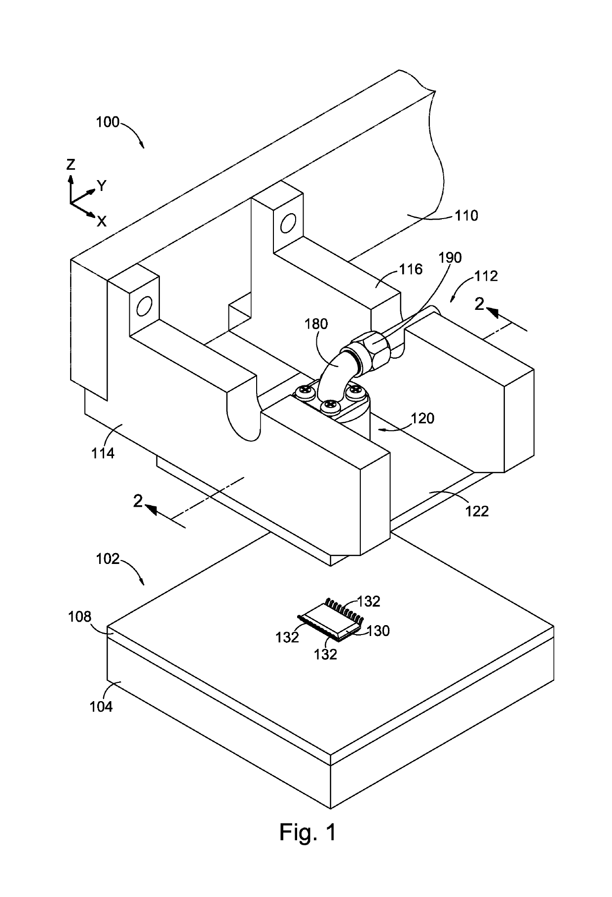
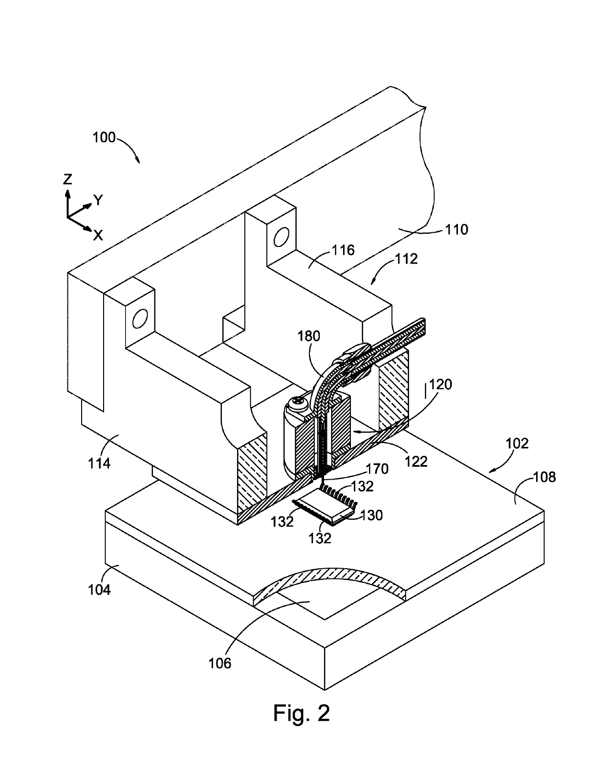
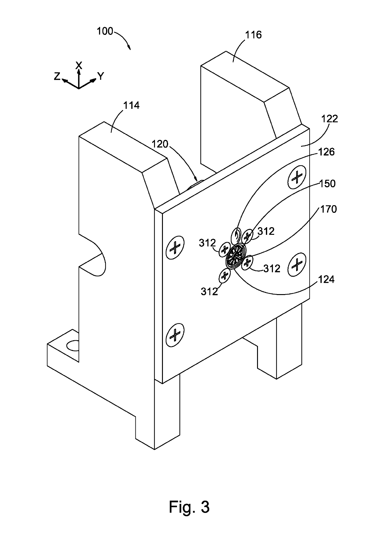
[0045]A current sensor having microwave chip resistors in parallel radial arrangement is disclosed in the attached drawings and is described below. The embodiment is disclosed for illustration of the current sensor having microwave chip resistors in parallel radial arrangement and is not limiting except as defined in the appended claims.

[0046]Most semiconductor integrated circuits (ICs) include electrostatic discharge (ESD) protection circuitry. Certain industry standards groups require testing of the protective circuitry for parts qualification. FIGS. 1-3 illustrate a schematic representation of portions of a CDM (charged device model) tester 100 into which the current sensor described herein may be incorporated. The CDM tester operates in a known conventional manner to measure the discharge of a charged device under test (DUT) when one of the leads of the DUT contacts a conductive material, which simulates an actual ESD threat.

[0047]Only the pertinent portions of the CDM tester 10...


PUM


Abstract

A current sensor for use with a charged device model (CDM) tester includes an outer conductor and a cylindrical inner conductor. The inner conductor is positioned within a central cylindrical bore of the outer conductor to provide a characteristic transmission line impedance of approximately 50 ohms. A test probe conductor extends from the distal end of the inner conductor and is electrically connected to the inner conductor. An array of self-supporting ceramic chip resistors is radially positioned between the distal ends of the inner conductor and the outer conductor to provide a uniformly distributed resistance between the inner conductor and the outer conductor. When the test probe conductor is applied to a pin of a charged device under test (DUT), a discharge current passes through the resistors and produces a voltage on the inner conductor that is provided as a signal voltage proportional to the discharge current.

Description

RELATED APPLICATIONS[0001]The present application claims the benefit of priority under 35 USC § 119(e) to U.S. Provisional Application No. 62 / 397,677, filed on Sep. 21, 2016, which is incorporated by reference herein.BACKGROUND OF THE INVENTIONField of the Invention[0002]This application is directed to systems for simulating electrostatic discharge (ESD) threats to semiconductor devices.Description of the Related Art[0003]To simulate electrostatic discharge (ESD) threats to semiconductors, a charged device model (CDM) tester provides a spark discharge to ground applied to each pin on an integrated circuit (IC). Four components of a CDM tester determine the waveform parameters: (1) the verification module; (2) the current sensor; (3) the oscilloscope; and (4) the coaxial cable carrying the discharge waveform from the current sensor to the oscilloscope.[0004]Present techniques for verifying CDM testers combine the time domain response tolerances of all four measurement components. Suc...

Claims


Application Information

Patent Timeline
Patent Type & Authority Patents(United States)
IPC IPC(8): G01R31/12G01R31/00H01C10/16G01R1/067G01R31/26
CPCG01R31/001H01C10/16G01R1/06722G01R1/06733G01R31/2607G01R15/247
Inventor BARTH, JON E.RICHNER, JOHN R.
Owner BARTH JON E
Why Eureka
Try Eureka