Structure for isolating high speed digital signals in a high density grid array

a high-density, grid array technology, applied in the direction of printed circuit manufacturing, printed circuit aspects, semiconductor/solid-state device details, etc., can solve the problem of high manufacturing cost, achieve unique signals, prevent metal layer trace damage, and mitigate cross-coupling of adjacent signals.

Active Publication Date: 2018-09-18
R&D CIRCUITS
View PDF5 Cites 0 Cited by
  • Summary
  • Abstract
  • Description
  • Claims
  • Application Information

AI Technical Summary

Benefits of technology

[0006]This present invention describes a structure implemented in a printed circuit board, in a printed circuit board sub-lamination, or in a like coplanar structure that mitigates cross-coupling of adjacent, unique signals, as defined by an integrated circuit grid array. The structure has three main components: (1) A micro-machined and plated isolation barrier connected to a supply voltage or ground, (2) Controlled depth drill removal of vias extending past the escape layers arranged in a sequenced pattern in the printed circuit board sub-lamination (or booklet) stack-up to prevent metal layer trace damage, and (3) A fine-pitch metal layer trace escape method that assists with impedance control.

Problems solved by technology

While the aforementioned prior art methods both work extremely well they require a high manufacturing cost.

Method used


Image

  • Structure for isolating high speed digital signals in a high density grid array
  • Structure for isolating high speed digital signals in a high density grid array
  • Structure for isolating high speed digital signals in a high density grid array

Examples


Embodiment Construction

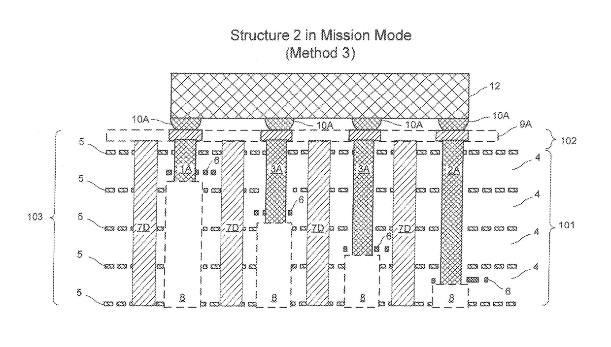
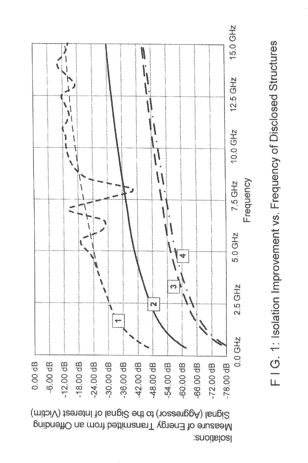
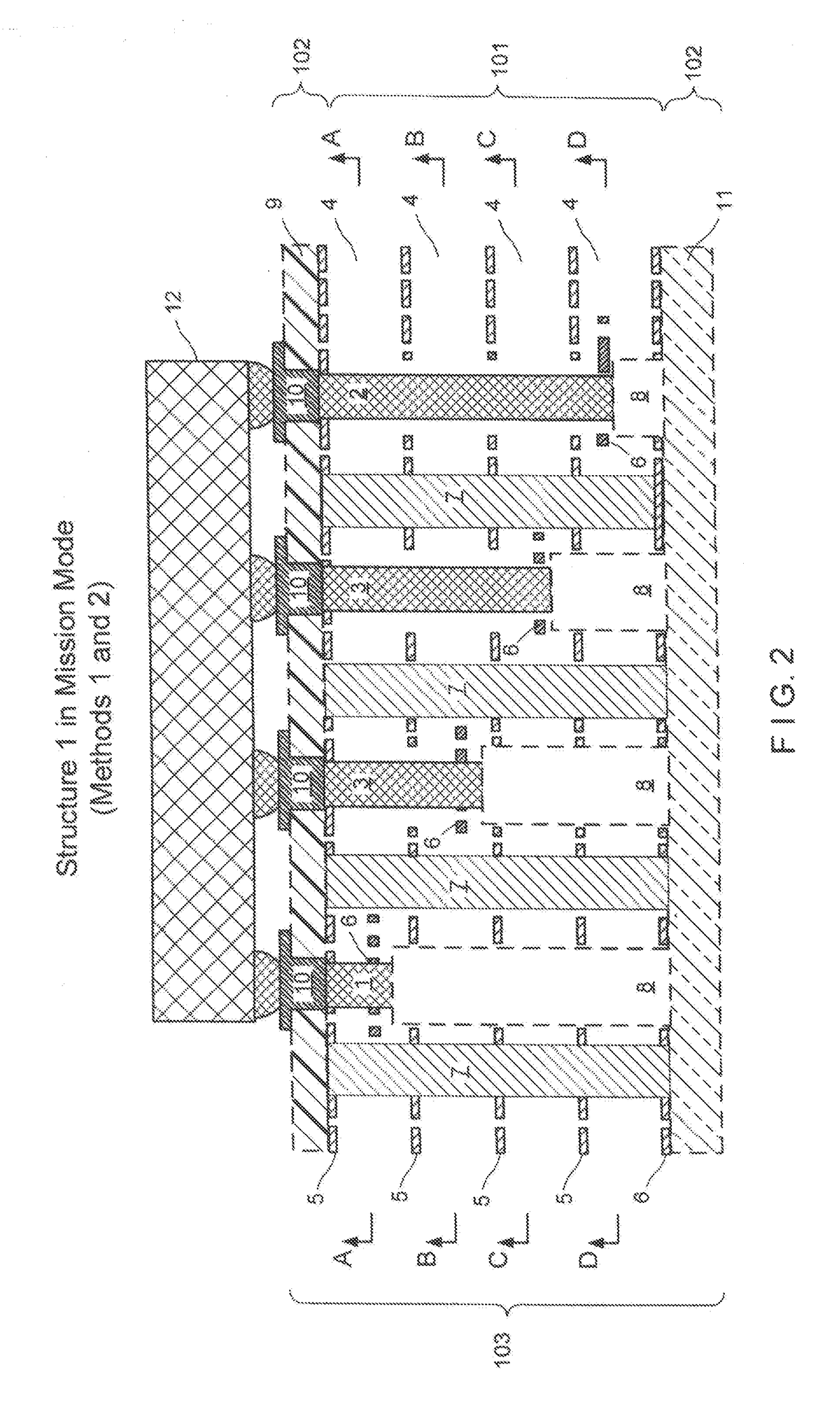
[0031]The present invention provides for three methods for isolating high speed digital signals in a high density grid array that utilize any one of a variety of isolation barrier shapes (element number 7) including round hole, c-shape, and straight line wall structures illustrated below respectively as element numbers 7a and 7b and 7c. Each of the isolation barriers 7, 7a, 7b, 7c and 7d can be used in two primary structures for any of the three methods. These two primary structures differ in how the isolation barrier is insulated from the integrated circuit device. The term mission mode in the present application refers to how the present invention operates when the integrated circuit device (IC) is connected.[0032]FIGS. 9-13 describe the first method for structure 1 with a nickel sintering paste mix or nickel plate. The element numbers for this embodiment are:[0033]1. Inner-most Integrated Circuit Device Escape via built into the sub-lamination[0034]2. Outer-most Integrated Circui...


PUM


Abstract

Due to size and cost, it becomes advantageous for integrated circuit (IC) manufacturers to use “single-ended” (one signal path per unique information path) high speed signals electrical contact pins (pins transmitting digital information that connect the integrated circuit to a printed circuit board) with a minimum number of surrounding powers and grounds. This lower cost method, however, creates electrical interference and coupling issues known as crosstalk between two adjacent signal paths in the via structure required to electrically connect the integrated circuit to the signal paths in the printed circuit board. Such crosstalk, in turn, increases jitter, degrades timing, and ultimately reduces the maximum operating speed of the circuit (performance). This disclosure presents a structure using micro-plating, micro-drilling and micro-machining methods that isolates adjacent signals by placing a metal barrier that shunts coupling currents to ground. The micro-drilling methods also reduce the length of adjacent signal paths in a specific signal routing and controlled depth drilling sequence.

Description

BACKGROUND[0001]1. Field[0002]This present invention is for a structure within a printed circuit board that is used for the purposes of mitigating electrical coupling (crosstalk) between two adjacent high speed signals. In particular the present invention relates to a structure implemented in a printed circuit board, in a printed circuit board sub-lamination, or in a like coplanar structure that mitigates cross-coupling of adjacent, unique signals, as defined by an integrated circuit grid array[0003]2. The Related Art[0004]Crosstalk issues are addressed by the prior art in one of two ways. Method one uses differential signals (two signal paths) for each unique information path. A differential signal escape with tight electrical coupling natively provides good isolation. Method two surrounds each electrical signal escaping the integrated circuit with a return current path (additional pin), such as electrical ground or electrical power. This isolation pin on the integrated circuit shu...

Claims


Application Information

Patent Timeline
Patent Type & Authority Patents(United States)
IPC IPC(8): H05K1/11H05K1/02H01L23/528H01L21/768H01L23/522H01L23/552
CPCH01L23/5225H01L23/5226H01L23/5286H01L23/552H05K1/0222H05K1/116H01L21/76843H05K2203/0207H01L2224/16225H05K1/0243H05K1/113H05K2201/0723H05K2201/09227H05K2201/09618H05K2201/09809H05K2201/10674H01L2223/6622H01L2224/16227H01L2924/15313H01L2924/3011
Inventor WARWICK, THOMAS P
Owner R&D CIRCUITS
Why Eureka
Try Eureka