
Lead mfg. method and method for shortening distance between lead an pattern

A technology of wire spacing and manufacturing method, which is applied in the manufacture of wires and narrows the distance between wires and patterns. It can solve problems such as deviation, inoperability of components, and decline in the overall performance and reliability of semiconductor components, so as to reduce the size of components and shrink the line width. Effect

Active Publication Date: 2007-06-13
NEXCHIP SEMICON CO LTD
View PDF0 Cites 3 Cited by
  • Summary
  • Abstract
  • Description
  • Claims
  • Application Information

AI Technical Summary

Problems solved by technology

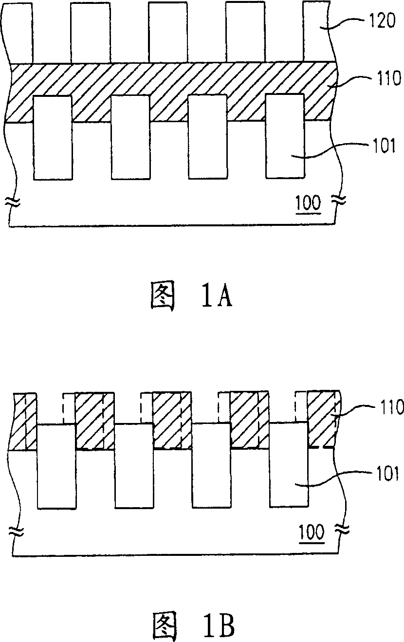
However, due to limitations in photolithography technology, the pattern of the polysilicon layer 110 may deviate due to overlay errors generated during the patterning of the photoresist layer, as shown by the dotted line in FIG. 1B shows that it cannot be accurately formed between two shallow trench isolations 101
This kind of error will cause abnormal electrical connection between word lines, or between word lines and components, which will lead to a significant decrease in the overall performance and reliability of semiconductor components, and may even cause the components to fail to operate.

Method used


Image

  • Lead mfg. method and method for shortening distance between lead an pattern
  • Lead mfg. method and method for shortening distance between lead an pattern
  • Lead mfg. method and method for shortening distance between lead an pattern

Examples


Embodiment Construction

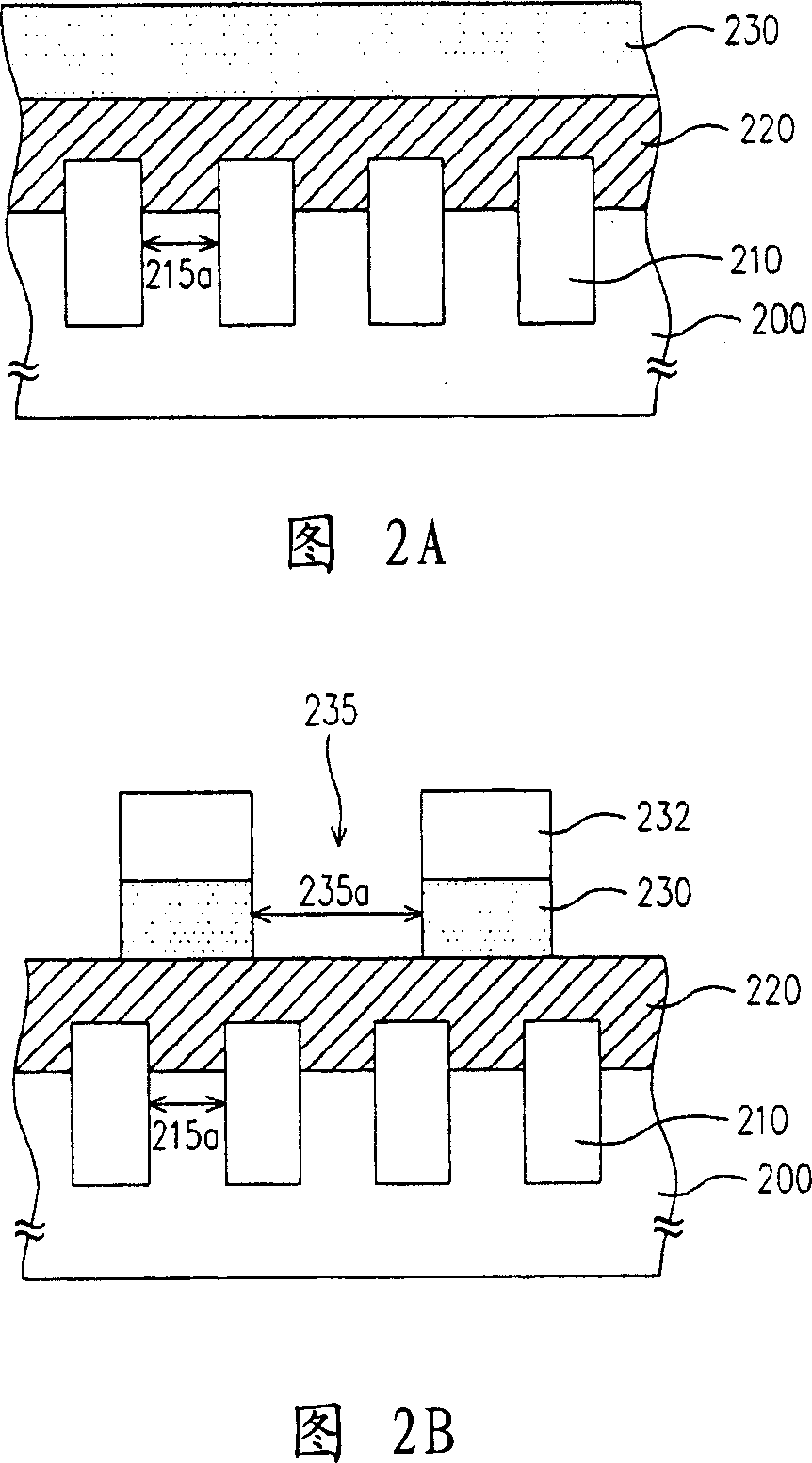
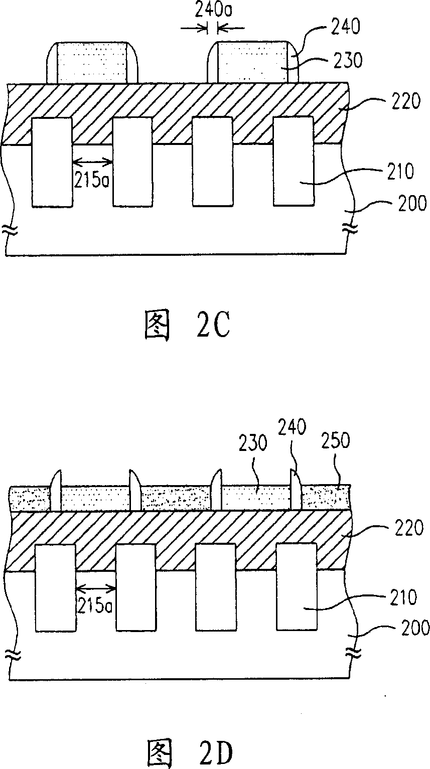
[0041] 2A to 2E are cross-sectional views illustrating a manufacturing process of a wire according to an embodiment of the present invention.

[0042] Referring to FIG. 2A , this embodiment is described by taking the formation of word lines of a memory as an example. Firstly, a substrate 200 having at least a plurality of isolation structures 210 is provided, and the surface of the substrate 200 may further include a dielectric layer (not shown). The isolation structure 210 is, for example, shallow trench isolation. According to the resolution of currently used photolithography machines, the width 215 a between the isolation structures 210 is, for example, 90 nm. Then, a layer 220 to be etched is formed on the substrate 200 . The layer to be etched 220 is, for example, a conductive layer, which is used as a subsequent control gate or wire. The material of the to-be-etched layer 220 is, for example, a conductive material such as doped polysilicon, metal or metal silicide, an...


PUM


Abstract

The method for reducing space between wires includes steps: providing substrate; forming first conductor layer on substrate; patternizing first conductor layer to form openings on the first conductor layer; forming gap walls on sidewall of the first conductor layer, and widths of these gap walls are smaller than widths of openings; on substrate, forming second conductor layer to be filled to the openings, and to expose top of each gap wall. Gap wall separates first conductor layer from second conductor layer. Width of gap wall is equal to space between first conductor layer and second conductor layer.

Description

technical field [0001] The invention relates to a semiconductor process, in particular to a method for manufacturing a wire on the semiconductor process and a method for reducing the distance between the wire and a pattern. Background technique [0002] Today, with the vigorous development of integrated circuits, the miniaturization and integration of components is an inevitable trend, and it is also an important topic for active development in the industry. The most important factor affecting the size of components in the entire semiconductor process lies in the technology of photolithography (Photolithography) process . [0003] In terms of the current semiconductor process technology, in order to further improve the resolution of the photolithography process, the machines, photomasks and even light sources used may be expensive. Moreover, under the condition that the accumulation degree of each component layout is increasing day by day, the overlay accuracy (Overlay Accu...

Claims


Application Information

Patent Timeline
IPC IPC(8): H01L21/768
Inventor 赖亮全王炳尧林诗绮
Owner NEXCHIP SEMICON CO LTD
Learn More