
Catastrophic transfer of thin film after co-implantation

A transfer method and thin-layer technology, which is applied in the fields of electrical components, microstructure technology, semiconductor/solid-state device manufacturing, etc., can solve problems such as no derivation, and achieve the effect of avoiding ring defects and improving topology

Active Publication Date: 2006-11-15
S O I TEC SILICON ON INSULATOR THECHNOLOGIES +1
View PDF3 Cites 2 Cited by
  • Summary
  • Abstract
  • Description
  • Claims
  • Application Information

AI Technical Summary

Problems solved by technology

But the article does not draw practical conclusions from it about the way to obtain high-quality thin layers at moderate cost, especially from the point of view of surface condition

Method used


Image

  • Catastrophic transfer of thin film after co-implantation
  • Catastrophic transfer of thin film after co-implantation
  • Catastrophic transfer of thin film after co-implantation

Examples


example

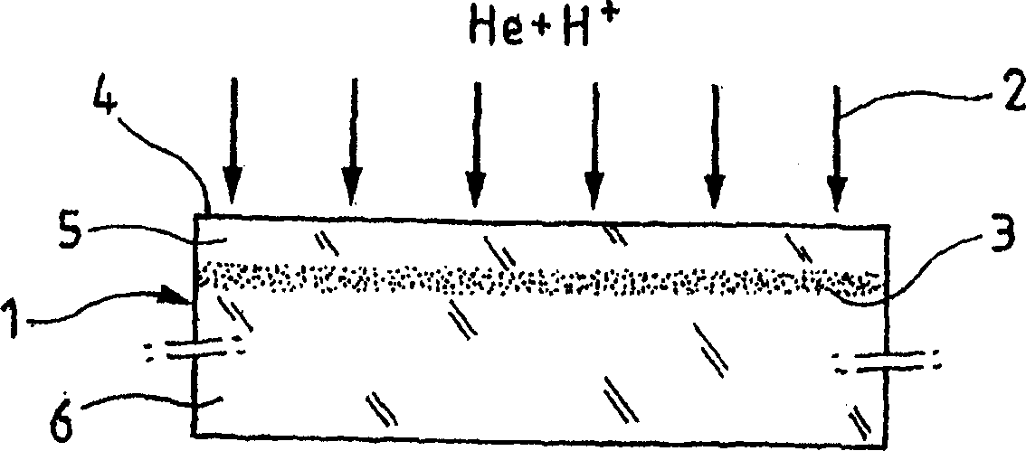
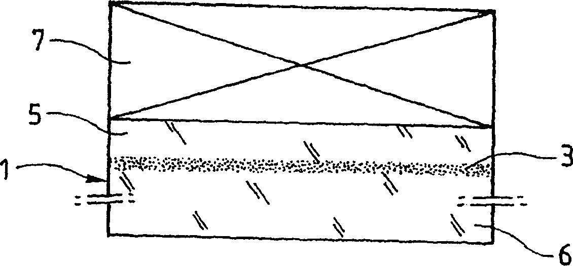
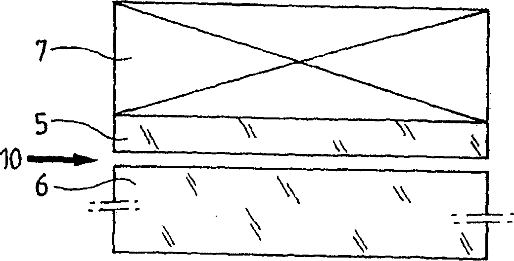
[0086] According to a first implementation example of the present invention, a surface (for example 145nm) contains a thermal SiO2 2 layer of Si substrate (-700μm) can be first at 70KeV-10 16 He / cm 2 Helium atoms are implanted under the implantation conditions, and then at 30KeV-4.25×10 16 H / cm 2 Hydrogen atoms were implanted under the implantation conditions. The source substrate can then be bonded to a target Si substrate (-700 μm) by direct bonding. A heat treatment around 350°C causes the increase of small disk-type cavities localized where the hydrogen concentration is maximum. There the helium atoms act as trapped atoms and generate the greatest number of small disk-type defects at the applied temperature. After a certain time (eg 2 hours), as soon as a blade is inserted between the bonded interfaces in the form of an impact, the catastrophic detachment of the hydrogen concentration maximum results in the transfer of a thin Si layer to the target substrate. The rou...


PUM


Abstract

The catastrophic transfer of a thin film comprises: - (a) preparing a source substrate; - (b) implanting a first species of ions or gas, in a first dose to a given depth, and a second species of ions or gas in a second dose, the first species being able to generate defects and the second species being able to occupy these defects; - (c) applying a stiffener in intimate contact with the source substrate; - (d) heat treating the source substrate to a given temperature for a given time, to create a buried fragile zone without initiating the thermal detachment of the thin film; and - (e) applying a localized energy contribution to provoke the catastrophic detachment of the thin film delimited between the surface and the buried fragile layer, this thin film having a surface with a rugosity below a given threshold.

Description

technical field [0001] The present invention relates to a method for the transfer of ultrathin layers (also called thin layers) at low temperatures by co-implantation. It is especially used in the fields of microelectronics, micromechanics, optics, and integrated electronics. Background technique [0002] As is known, detachment of the thin layer can be achieved by implanting chemical species into the source substrate (eg, composed of silicon) to induce the formation of a defect region at a certain depth. These defects may be microscopic bubbles and / or platelets and / or microscopic cavities and / or misplaced rings and / or other crystal defects, thereby locally disturbing the crystalline quality of the material; their characteristics, density, size are greatly dependent on Depends on the species being implanted (typically, hydrogen) and the properties of the source substrate. A heat treatment can then be applied to allow the development of specific defects present in the weake...

Claims


Application Information

Patent Timeline
IPC IPC(8): H01L21/762B81C99/00
CPCH01L21/76254H01L21/265H01L21/762H01L21/30H01L21/46
Inventor 纳古耶特-福恩格·纳古耶恩伊恩·凯瑞福克克里斯蒂尔·拉加赫-布兰查德
Owner S O I TEC SILICON ON INSULATOR THECHNOLOGIES
Learn More