
Double-colour indium-gallium-arsenide infrared detector and producing method and application thereof

An infrared detector, indium gallium arsenic technology, applied in semiconductor devices, final product manufacturing, sustainable manufacturing/processing, etc., can solve the problem of large volume and weight of the infrared detection system, high power consumption of the detection system, low cost performance, etc. problem, to achieve the effect of light weight, improved anti-interference, and small size

Inactive Publication Date: 2006-10-18
SOUTH CHINA NORMAL UNIVERSITY
View PDF0 Cites 11 Cited by
  • Summary
  • Abstract
  • Description
  • Claims
  • Application Information

AI Technical Summary

Problems solved by technology

At present, the main disadvantages of infrared detection technology are: (1) a cooling system needs to be manufactured to ensure the normal operation of the infrared detector; (2) the entire infrared detection system is large in size and weight; (3) the power consumption of the detection system is high; (4) ) Low cost performance, and extremely inconvenient to use; (5) A device can only detect one wavelength information

Method used


Image

  • Double-colour indium-gallium-arsenide infrared detector and producing method and application thereof
  • Double-colour indium-gallium-arsenide infrared detector and producing method and application thereof
  • Double-colour indium-gallium-arsenide infrared detector and producing method and application thereof

Examples


Embodiment Construction

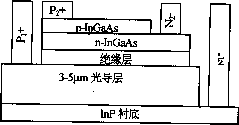
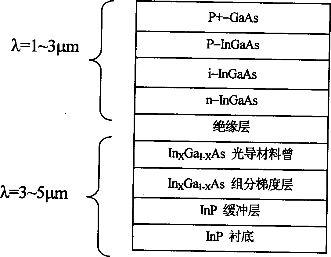
[0025] Adopt the method of the present invention to prepare two-color InGaAs infrared detector: form InP buffer layer, InP buffer layer, InP substrate with epitaxy method x Ga 1-x As composition gradient layer, In x Ga 1-x As photoconductive material layer and other structures; continue to grow the insulating layer, and then use the epitaxy method to form N-type-InGaAs layer, I-type-InGaAs layer, P-type-InGaAs layer, P+ electrode-GaAs layer and other structures. get figure 2 Infrared epitaxial wafer layers shown.

[0026] After the epitaxial wafer is grown by the epitaxial method, the surface of the N-type layer is etched using the semiconductor planar process technology, photolithography and chemical etching, and then the ohmic contact electrode pattern of the N-type layer is formed by photolithography. The evaporation method evaporates the N-type layer ohmic contact electrode, and the P-type layer ohmic contact electrode can be made in the same way, that is, the manufac...


PUM


Abstract

The present invention relates to a two-color InGaAs infrared detector. It is characterized by that on the InP substrate are successively grown a photoconductive layer which has InxGa1-x As material and is suitable for detecting 3-5 micrometer infrared wave, an insulating layer and an InGaAs material layer which has PIN structure and is suitable for detecting 1-3 micrometer infrared wave. Said invention also provides the concrete steps of its preparation method, and said infrared detector can be used for preparing the device for multiway measuring infrared signal.

Description

technical field [0001] The invention relates to semiconductor technology, and mainly relates to a two-color indium gallium arsenide (InGaAs) infrared detector with a photoconductive material and a PIN structure grown on a substrate. [0002] The invention also relates to a preparation method of the infrared detector. [0003] The invention also relates to the application of said infrared detector. technical background [0004] Infrared detector technology has been developed rapidly, but most infrared detectors need to work at low temperature to obtain high performance, such as: mercury cadmium telluride, pyroelectric release, germanium silicon, aluminum gallium arsenic / gallium arsenic, platinum silicon, etc. Due to the need for refrigeration, the infrared system is bulky, heavy, expensive and unfavorable to use, which affects their wide application. Therefore, refrigeration is the main obstacle to the widespread application of infrared detectors. In the past ten years, peo...

Claims


Application Information

Patent Timeline
IPC IPC(8): H01L31/08H01L31/18
CPCY02P70/50
Inventor 孙慧卿范广涵郭志友
Owner SOUTH CHINA NORMAL UNIVERSITY
Learn More