


Quick Research
Generate reliable direction feasibility study reports for your R&D in just a few steps.

Technical Q&A
Discover and master advanced knowledge NOW. Basics, ideas, possibilities, all at once.

Find Solutions
As an expert in R&D theories, this can generate solutions to your technical problems instantly.

Evaluate Feasibility
Analyze your overall solution with one click, know your potential R&D risks in advance.

Monitor Landscape
Get weekly tech updates, stay abreast of the latest tech innovations and key insights.
Organic thin film transistor and manufacturing method thereof
A technology of organic thin film and production method, applied in semiconductor/solid-state device manufacturing, electric solid-state device, semiconductor device, etc., can solve the problem of insufficient surface roughness, and achieve the effect of stable working characteristics
- Summary
- Abstract
- Description
- Claims
- Application Information
AI Technical Summary
Problems solved by technology
Method used
Image


Examples
example 1
[0061] Figure 4-8 It is a schematic diagram of the fabrication method of the organic thin film transistor of the present invention. exist Figure 4 In, reference numeral 401 denotes a substrate, and 402 denotes a conductor film. As for the substrate 401 and the conductor film 402, for example, a glass epoxy substrate integrated with copper foil, that is, a commercially available printed circuit board. In this example, a substrate having a thickness of 0.2 mm in which a copper foil (produced by Hitachi Chemical Co., Ltd., model: FR-4) having a thickness of 35 µm as a conductor film was used. A large number of substrates are structured with conductive films on both sides. However, according to the description of the present invention, it is not necessary to have a conductor film on one surface, so it is omitted here. exist Figure 4-8 The same reference numerals denote the same parts.
[0062] Next, the conductor film is patterned so that it becomes a desired gate shape. ...
example 2
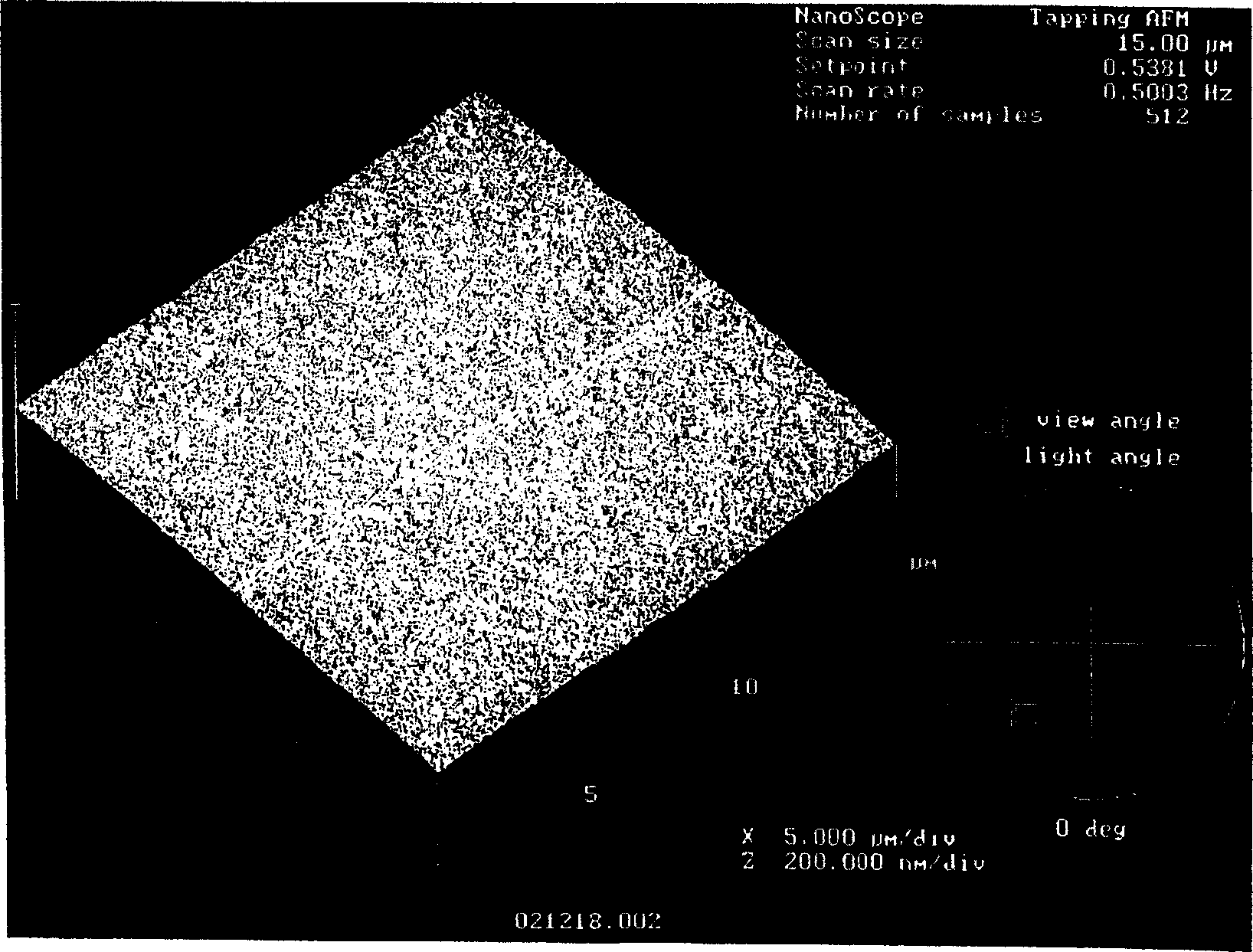
[0075] An organic thin film transistor was fabricated as in Example 1, except that polyethylene terephthalate (PET) was used as the substrate and gold was used as the gate electrode. For organic thin film transistors, the relationship between the average surface roughness Ra of the gate electrode surface and the defective rate was examined.
[0076] The PET used was an OHP film, 0.1 mm thick, A4 size. It was cut to the card size (86mm x 54mm) as in Example 1.
[0077] The gold film that will later become the gate electrode is fabricated in a vacuum evaporation system using a resistively heated tungsten boat and using a mask. In order to improve the contact between the gold film and the substrate, a thin chromium film is made as the bottom layer first. The thickness of the gold film was 0.5 μm, and the thickness of the chromium film was 0.1 μm.
[0078] Next, the laminated film of the chromium film and the gold film to be the gate electrode is polished by CMP. Adjust the po...
example 3
[0082] A 25 μm thick polyimide sheet was used as the organic substrate. Copper foil with a thickness of 25 μm is plated on the substrate. Four substrates grown with copper foil were prepared.
[0083] These four substrates were subjected to four surface treatments: unpolished, soft-etched, polished tape, and CMP.
[0084] The conditions of each surface treatment are as follows.
[0085] (processing conditions)
[0086] Soft corrosion treatment: immerse the substrate in 5% sulfuric acid for 30 seconds, and then rinse it with flowing deionized water for 2 minutes.
[0087] Polishing belt treatment: polishing belt (model: K8000); polishing time 60 seconds; belt feeding speed 1m / 30 seconds; roller pressure 2kgf / cm 2 .
[0088] CMP treatment: Shibaura polishing fluid CHS-3000EM; cylinder pressure 5kg; polishing tray and polishing disk rotation speed 80rpm; polishing time 25 minutes.
[0089] Each of the above-treated substrates was cut into a square size of 17 mm. Then, the ...
PUM
 Abstract
Description
Claims
Application Information
 - R&D Engineer
- R&D Manager
- IP Professional
- Industry Leading Data Capabilities
- Powerful AI technology
- Patent DNA Extraction
Browse by: Latest US Patents, China's latest patents, Technical Efficacy Thesaurus, Application Domain, Technology Topic, Popular Technical Reports.
© 2024 PatSnap. All rights reserved.Legal|Privacy policy|Modern Slavery Act Transparency Statement|Sitemap|About US| Contact US: help@patsnap.com