Method and apparatus employing integrated metrology for improved dielectric etch efficiency

A technology of equipment and measurement values, applied in semiconductor/solid state device testing/measurement, circuits, electrical components, etc., to solve the problem of inability to monitor wafer etching uniformity by interferometric sensors, interferometric sensors that cannot be monitored or corrected, and improper chip etching And other issues

Inactive Publication Date: 2005-12-21
APPLIED MATERIALS INC
View PDF2 Cites 10 Cited by
  • Summary
  • Abstract
  • Description
  • Claims
  • Application Information

AI Technical Summary

Problems solved by technology

Also, since only the center die is seen by the sensor, it is not possible to monitor etch uniformity across the wafer with interferometric sensors
So off-center chips may be etched improperly, and interferometric sensors cannot monitor or correct for this situation

Method used


Image

  • Method and apparatus employing integrated metrology for improved dielectric etch efficiency
  • Method and apparatus employing integrated metrology for improved dielectric etch efficiency
  • Method and apparatus employing integrated metrology for improved dielectric etch efficiency

Examples


Embodiment Construction

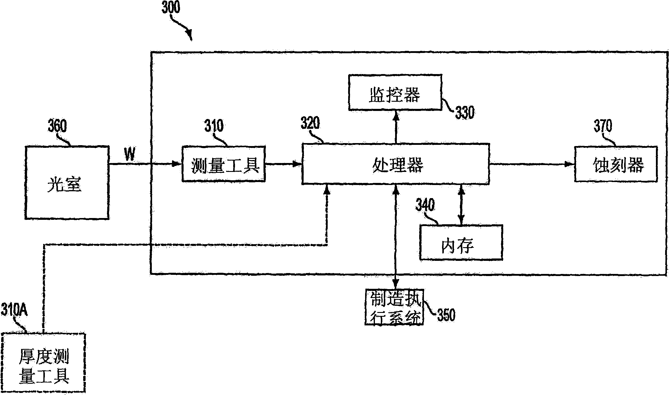
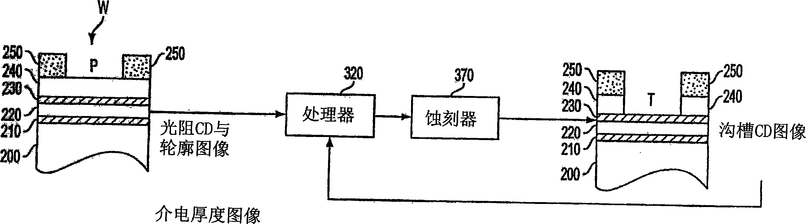
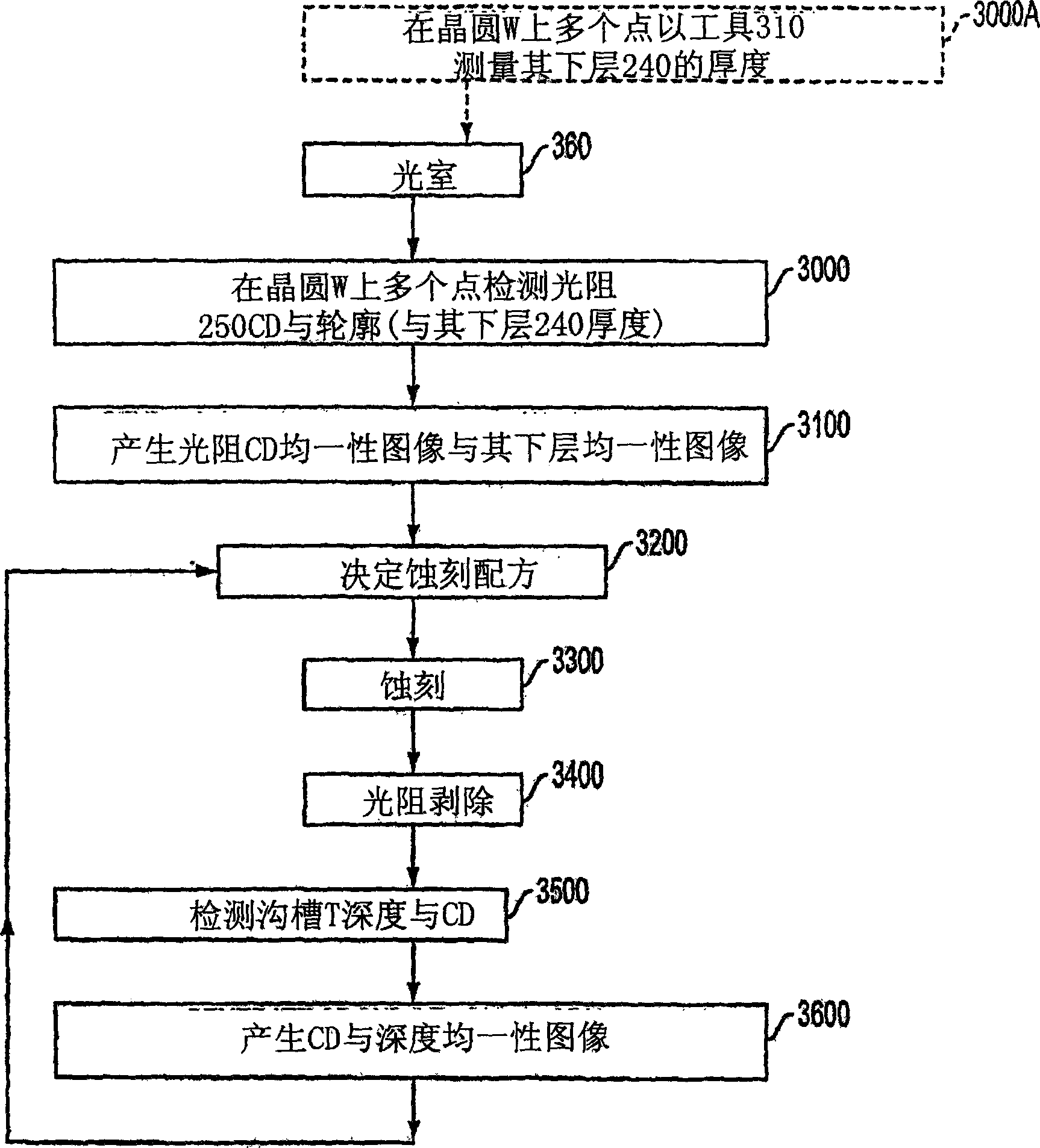
[0040] The traditional measurement method for detecting the features formed on the surface of the semiconductor wafer during the manufacturing process cannot effectively analyze the error between the CD and / or the outline and the design rules, so as to provide early information for positively identifying the source of the defect, or to carry out the process control to reduce size variation. The present invention solves the CD control problem by reducing the CD variation by feeding back information about the CD and profile of the photoresist mask, and measuring the thickness of the underlying layer at multiple points on the wafer to adjust the next process of the inspected wafer ( such as etching process). In some embodiments of the present invention, CD, profile and thickness measurement, etch processing and post-etch cleaning are performed in a single module in a controlled environment, thereby increasing throughput and improving yield. The present invention provides a self-...


PUM


Abstract

The present invention provides a method and equipment for processing semiconductor wafers to reduce dimensional changes. It measures the CD and profile of the photoresist mask and the thickness of the underlying layer at multiple points on the wafer and feeds back such information to adjust the following A process (eg, etch process) of the inspected wafer to be processed. After this processing step, the dimensions of the features formed by the process, such as the CD and depth of the trenches, are measured at multiple points on the wafer and this information is fed back to the processing tool to adjust the process for the next wafer , further reducing size variations. In some embodiments, CD, profiling, thickness and depth measurements, etch processing and post-etch cleaning are performed in a single module in a controlled environment. All transfer and processing steps implemented by this module are carried out in a clean environment, thereby avoiding exposure of the wafer to the atmosphere and avoiding possible contamination between steps to increase yield.

Description

technical field [0001] The present invention relates to methods and apparatus for monitoring and controlling processes performed on semiconductor substrates, and in particular, feedback and feedback information collected during feature inspection for controlling features formed on semiconductor substrates Contour and critical dimension (CD) uniformity. The present invention has particular applicability to in-line inspection of semiconductor wafers during the fabrication of high density semiconductor components with sub-micron features. Background technique [0002] Today's high density and performance requirements for VLSI require sub-micron features, increased transistor and circuit speed, and improved reliability. Such demands require highly accurate and uniform formation of component features, necessitating careful process monitoring, including frequent and detailed inspection of components while the features are still in semiconductor wafer form. [0003] A conventiona...

Claims


Application Information

Patent Timeline
Patent Type & Authority Applications(China)
IPC IPC(8): H01L21/66
CPCH01L22/20H01L2924/0002H01L2924/00H01L22/00
Inventor 季米特里斯·林贝罗普洛斯加里·苏尔苏克希·莫汉
Owner APPLIED MATERIALS INC
Why Eureka
Try Eureka