Electromagnetic shielding sheet and method for manufacturing same
An electromagnetic wave and sheet technology, which is applied in the fields of magnetic/electric field shielding, chemical instruments and methods, electrical components, etc., can solve the problems of reduced blackness of electromagnetic wave shielding sheets, insufficient visibility of display images, and poor electromagnetic wave shielding performance, etc., to achieve Emphasis on the effect of excellent effect, excellent light absorption, and high durability
- Summary
- Abstract
- Description
- Claims
- Application Information
AI Technical Summary
Problems solved by technology
Method used
Image
Examples
Embodiment 1
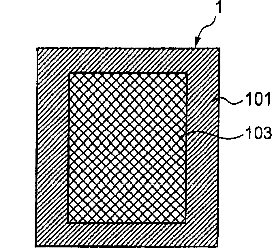
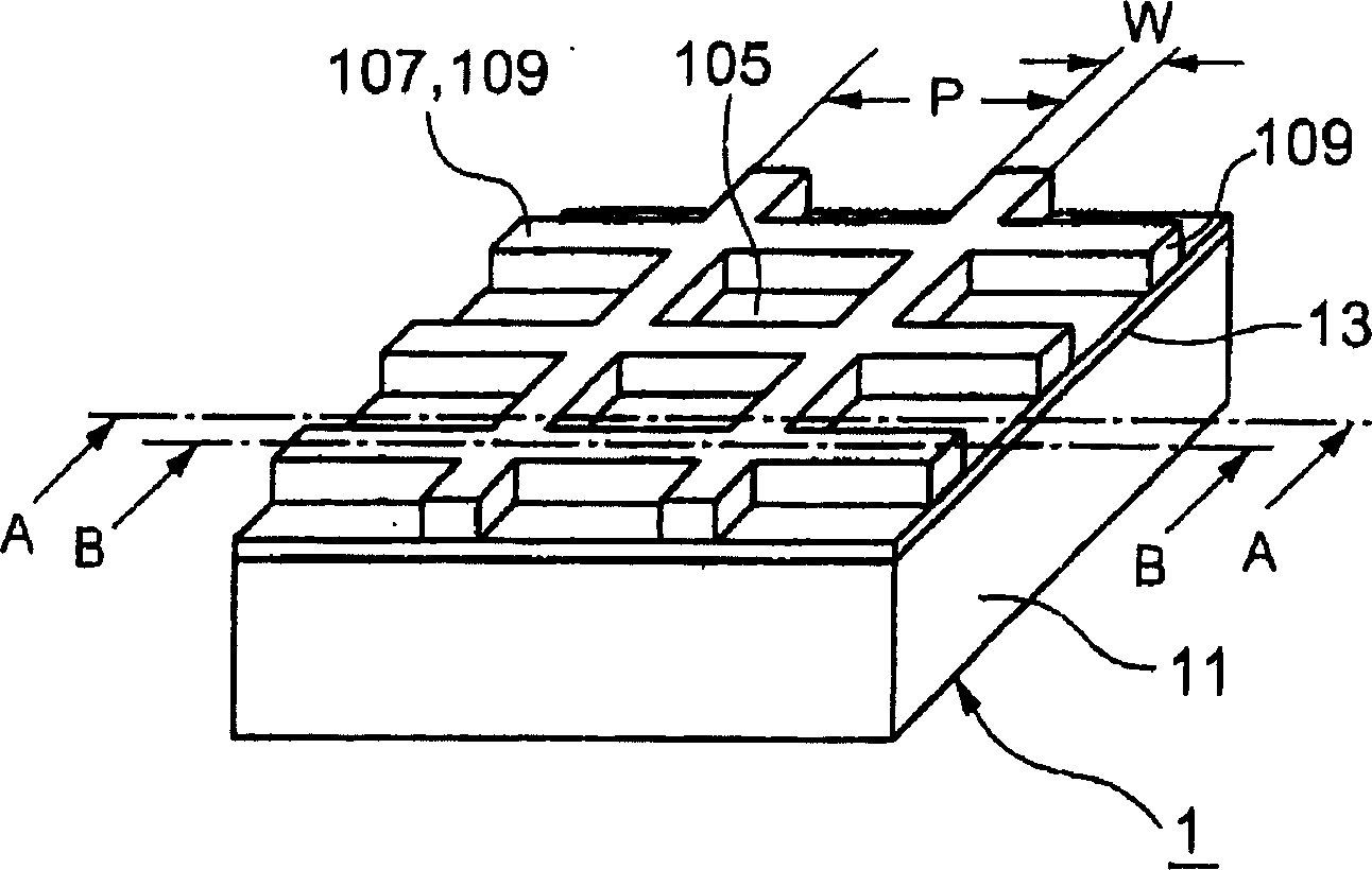
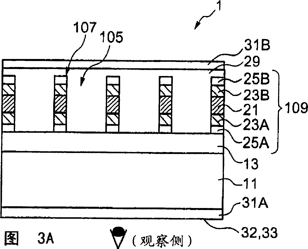
[0133]As a conductive material layer containing a metal layer, an electrolytic copper foil for forming the metal layer 21 is prepared, and copper-cobalt alloy particles (average particle diameter: 0.3 μm) are subjected to cathodic electrodeposition on both surfaces to form blackened layers 23A, 23B. , and then carry out chromate treatment on its surface to make a blackened strengthening layer. The thickness of the metal layer is 10 μm, and the surface of the copper-cobalt alloy particles and chromate treatment is implemented, and a biaxially stretched polyethylene terephthalate (PET) film A4300 (manufactured by Toyobo Co., Ltd., trade name) with a thickness of 100 μm is ), laminated with a two-component curing polyurethane adhesive, and then aged at 56°C for 3 days. As the adhesive, the main agent TAKERAKKU A-310 (polyalcohol) composed of polyalcohol and the curing agent A-10 composed of polyisocyanate (both manufactured by Takeda Pharmaceutical Co., Ltd., trade name) are used...
Embodiment 2
[0146] A flat layer composition of the following composition was applied to the mesh of Example 1, and SP-PET20-BU (manufactured by Tosero Corporation, trade name of PET film with surface release treatment) was laminated to a thickness of 50 μm. cm 2 Exposure (converted to 365nm). And when SP-PET20-BU was peeled, the sheet|seat for electromagnetic wave shields of Example 2 in which the mesh part was flattened was obtained. This electromagnetic wave shielding sheet had the same performance as that of Example 1.
[0147] The flat layer composition used: 20 parts by mass of N-vinyl-2-pyrrolidone, 25 parts by mass of dicyclopentenyl acrylate, 52 parts by mass of oligoester acrylate (manufactured by Toagosei Co., Ltd., M-8060), 3 parts by mass of 1-hydroxycyclohexyl phenyl ketone (manufactured by ciba-Geigy, IRUGACURE 184).
Embodiment 3
[0149] A sheet for electromagnetic shielding was obtained in the same manner as in Example 2 except that 1 part by mass of a nickel thiol complex was contained as an NRI absorber in the flat layer composition of Example 2. This electromagnetic wave shielding sheet had the same performance as that of Example 1, and the visibility of the display image was better.
PUM
| Property | Measurement | Unit |
|---|---|---|
| particle diameter | aaaaa | aaaaa |
| wavelength | aaaaa | aaaaa |
| diameter | aaaaa | aaaaa |
Abstract
Description
Claims
Application Information
 - R&D Engineer
- R&D Manager
- IP Professional
- Industry Leading Data Capabilities
- Powerful AI technology
- Patent DNA Extraction
Browse by: Latest US Patents, China's latest patents, Technical Efficacy Thesaurus, Application Domain, Technology Topic, Popular Technical Reports.
© 2024 PatSnap. All rights reserved.Legal|Privacy policy|Modern Slavery Act Transparency Statement|Sitemap|About US| Contact US: help@patsnap.com


