


Quick Research
Generate reliable direction feasibility study reports for your R&D in just a few steps.

Technical Q&A
Discover and master advanced knowledge NOW. Basics, ideas, possibilities, all at once.

Find Solutions
As an expert in R&D theories, this can generate solutions to your technical problems instantly.

Evaluate Feasibility
Analyze your overall solution with one click, know your potential R&D risks in advance.

Monitor Landscape
Get weekly tech updates, stay abreast of the latest tech innovations and key insights.
Method for making T type grating through combination of X-ray etching and optical etching
An X-ray and lithography technology, which is used in the field of mixing X-ray lithography and optical lithography to make T-shaped gratings, can solve the problems that the electron beam time cannot be adapted to large-scale production, and the electron beam lithography is complicated.
- Summary
- Abstract
- Description
- Claims
- Application Information
AI Technical Summary
Problems solved by technology
Method used
Image


Examples
Embodiment
[0026] Such as diagram 2-1 As shown, first coat the underlying X-ray photoresist 202 on the PHEMT or MESFET chip 201, the thickness of the photoresist is between 150-300nm, and the photoresist 202 can be PMMA or ZEP 520 or UVIII.
[0027] Such as Figure 2-2 As shown, the X-ray lithography method exposes the underlying X-ray photoresist 202 .
[0028] Such as Figure 2-3 As shown, the top layer of optical photoresist 203 is coated. The optical photoresist can be S9912 or I-line adhesive, and the thickness of the adhesive is 1000-1500 nm.
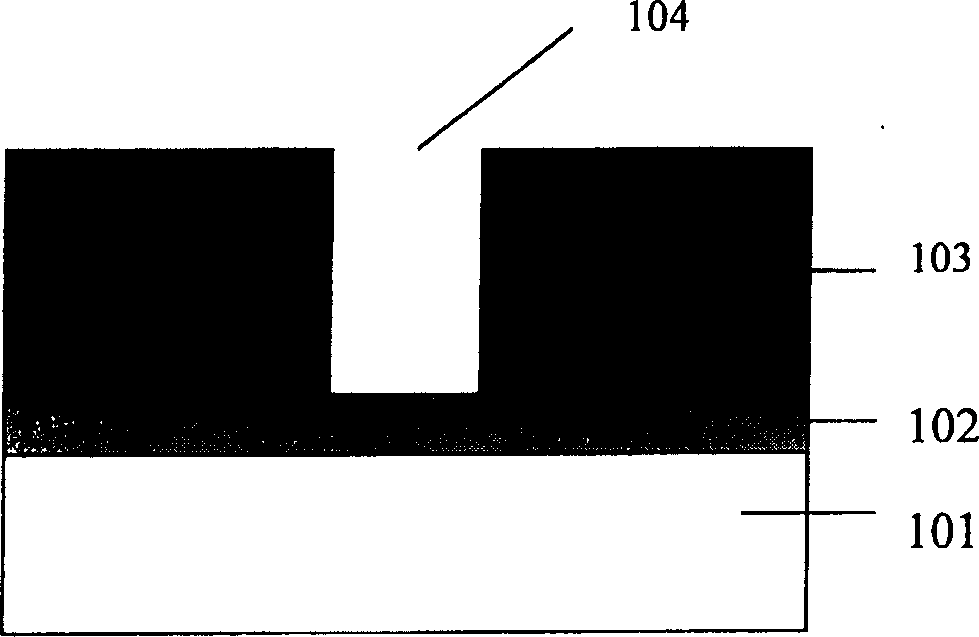
[0029] Such as Figure 2-4 As shown, the photolithography method exposes the top photoresist, and develops the top photoresist to obtain the wide gate pattern 204 .
[0030] Such as Figure 2-5 As shown, develop the underlying X-ray photoresist to obtain the gate groove pattern 205, use oxygen plasma to prime the glue for 40 seconds, and the oxygen flow rate is 20 sccm, then soak in phosphoric acid: deionized water=1:10 for 50 seconds,...
PUM
| Property | Measurement | Unit |
|---|---|---|
| Thickness | aaaaa | aaaaa |
Abstract
Description
Claims
Application Information
 - R&D Engineer
- R&D Manager
- IP Professional
- Industry Leading Data Capabilities
- Powerful AI technology
- Patent DNA Extraction
Browse by: Latest US Patents, China's latest patents, Technical Efficacy Thesaurus, Application Domain, Technology Topic, Popular Technical Reports.
© 2024 PatSnap. All rights reserved.Legal|Privacy policy|Modern Slavery Act Transparency Statement|Sitemap|About US| Contact US: help@patsnap.com