High precison femtosecond synchronous technology and device
A femtosecond laser and synchronization device technology, applied in the field of femtosecond laser synchronization technology and devices, can solve problems such as low synchronization accuracy, achieve the effects of narrow pulse width, avoid gain competition effect, and high synchronization accuracy
- Summary
- Abstract
- Description
- Claims
- Application Information
AI Technical Summary
Problems solved by technology
Method used
Image
Examples
Embodiment 1
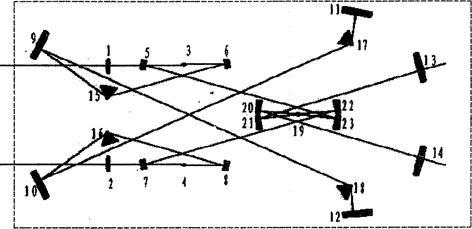
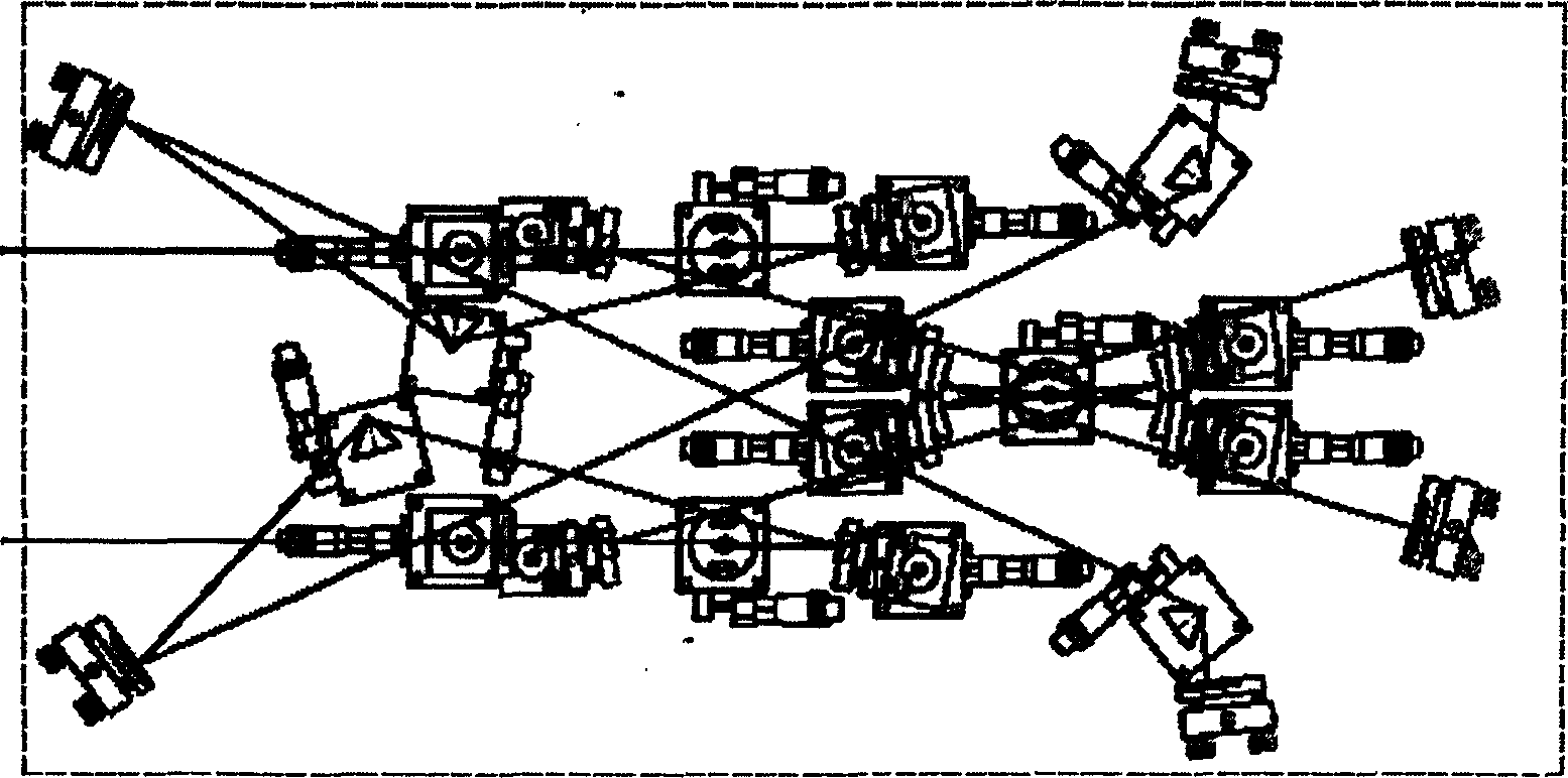
[0030] Such as image 3 shown, where each element is associated with figure 1 Correspondingly, all are installed on the base plate with a size of 800×400mm. The specific parameters and installation requirements for component selection are as follows:
[0031]Put the focusing lenses 1 and 2 on the adjustment frame that can adjust the lifting and left and right positions, and place the adjustment frame on the 40×40mm translation platform, and the plano-concave mirrors 5 and 7 are located on the two-dimensional adjustable fine-tuning frame , while the other plano-concave full mirror 6, 8 is located on the two-dimensionally adjustable fine-tuning frame and the translation stage of 40 × 40mm. The laser crystals 3 and 4 are located on the crystal adjustment frame and the horizontal rotating table that can adjust the pitch and angle. The two ends of the adjustment frame are connected to the water cooling cycle with rubber tubes, and the rotating crystals are respectively placed on t...
Embodiment 2
[0037] The specific parameters and installation of each element are as in embodiment 1. However, 13 and 14 are used as planar total reflection mirrors, and a K9 glass substrate with a diameter of 25.4mm and a thickness of 4mm is coated with a broadband dielectric film that is fully reflected at 700-900nm under normal incidence; 11 and 12 are used as planar output mirrors, and A fused silica substrate with a diameter of 25.4mm and a thickness of 4mm is coated with a dielectric film with a transmittance of 10%-20% in the 750-850nm band under normal incidence.
Embodiment 3
[0039] The specific parameters and installation of each element are as in embodiment 1. However, the coupling crystal 19 is a quartz crystal with a thickness of 5 mm and a Brewster angle cut.
PUM
 Abstract
Description
Claims
Application Information
 - R&D
- Intellectual Property
- Life Sciences
- Materials
- Tech Scout
- Unparalleled Data Quality
- Higher Quality Content
- 60% Fewer Hallucinations
Browse by: Latest US Patents, China's latest patents, Technical Efficacy Thesaurus, Application Domain, Technology Topic, Popular Technical Reports.
© 2025 PatSnap. All rights reserved.Legal|Privacy policy|Modern Slavery Act Transparency Statement|Sitemap|About US| Contact US: help@patsnap.com


