Composite substrate material of conductive spinel structure MgIn2O4/MgO and its prepn

A composite substrate and spinel-type technology, applied in semiconductor/solid-state device manufacturing, circuits, electrical components, etc., can solve the problems of increasing device volume, less use, waste of raw materials, etc., and achieve simple preparation process and easy operation Effect

Inactive Publication Date: 2004-09-08
SHANGHAI INST OF OPTICS & FINE MECHANICS CHINESE ACAD OF SCI
View PDF0 Cites 3 Cited by
  • Summary
  • Abstract
  • Description
  • Claims
  • Application Information

AI Technical Summary

Problems solved by technology

[0009] (2) Since the lattice mismatch between MgO crystal and GaN reaches 13%, and it is not stable enough in MOCVD atmosphere, it is less used;
[0010] (3) The above transparent oxide substrates are not conductive, making the device difficult to manufacture, and also increases the volume of the device, resulting in a lot of waste of raw materials

Method used


Image

  • Composite substrate material of conductive spinel structure MgIn2O4/MgO and its prepn
  • Composite substrate material of conductive spinel structure MgIn2O4/MgO and its prepn

Examples


Embodiment Construction

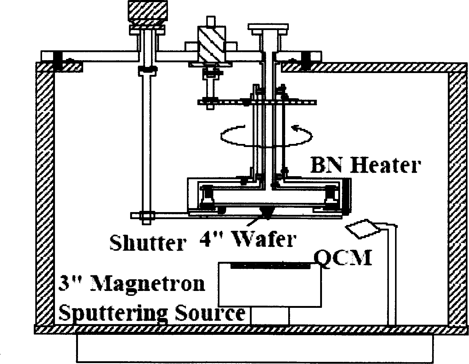
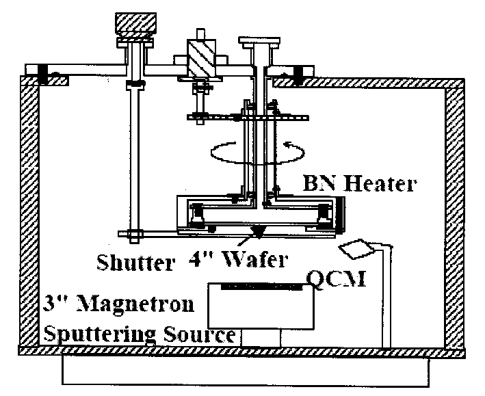
[0030] figure 1 is a schematic diagram of the magnetron sputtering apparatus. The sputtering mechanism is Ar + Accelerated by an electric field, it becomes a high-energy incident particle that hits In 2 o 3 The target material transfers part of the momentum to the target atom, and the target atom collides with other target atoms to form a cascade process. In this cascade process, some target atoms near the surface obtain enough momentum to move outward and leave the target. It is sputtered out, falls on the MgO single crystal substrate placed a few centimeters away from the surface of the target, adheres and accumulates to deposit In 2 o 3 film. In the usual sputtering method, the sputtering efficiency is not high, adding a magnetic field can increase the ionization efficiency of argon (Ar), thereby improving the sputtering efficiency.

[0031] The radio frequency magnetron sputtering technique of the present invention prepares composite substrate material MgIn 2 o 4 T...


PUM


Abstract

The composite substrate material of conductive spinel structure MgIn2O4 / MgO is constituted via setting one layer of covering MgIn2O4 layer onto the monocrystalline MgO. The preparation process of the composite substrate material includes the first RF magnetically controlled sputtering to prepare In2O3 film on monocrystalline MgO substrate, and the subsequent solid reaction between In2O3 and MgO at high temperature to form covering MgIn2O4 layer on the monocrystalline MgO substrate. The composite substrate material of the present invention has simple preparation process, and MgIn2O4 has small lattice mismatching degree to GaN (111) and is transparent conducting oxide material. The composite MgIn2O4 / MgO substrate is suitable for epitaxial growth of high quality GaN.

Description

technical field [0001] The invention relates to a conductive spinel structure MgIn suitable for epitaxial growth of InN-GaN-based blue light semiconductors 2 o 4 / MgO composite substrate material and its preparation method. Background technique [0002] Wide bandgap III-V compound semiconductor materials represented by GaN are receiving more and more attention, and they will be used in blue and green light-emitting diodes (LEDs) and laser diodes (LDs), high-density information reading and writing, underwater It has broad application prospects in communication, deep water exploration, laser printing, biological and medical engineering, as well as ultra-high-speed microelectronic devices and ultra-high-frequency microwave devices. [0003] Due to GaN's high melting point, high hardness, and high saturated vapor pressure, high temperature and high pressure are required to grow large-sized GaN bulk single crystals. The Polish High Pressure Research Center only produced strips ...

Claims


Application Information

Patent Timeline
IPC IPC(8): H01L21/02H01L21/84H01L33/00
Inventor 徐军彭观良周圣明周国清杭寅李抒智杨卫桥赵广军王海丽刘军芳李红军吴锋王静雅司继良庄漪邹军
Owner SHANGHAI INST OF OPTICS & FINE MECHANICS CHINESE ACAD OF SCI
Why Eureka
Try Eureka