


Quick Research
Generate reliable direction feasibility study reports for your R&D in just a few steps.

Technical Q&A
Discover and master advanced knowledge NOW. Basics, ideas, possibilities, all at once.

Find Solutions
As an expert in R&D theories, this can generate solutions to your technical problems instantly.

Evaluate Feasibility
Analyze your overall solution with one click, know your potential R&D risks in advance.

Monitor Landscape
Get weekly tech updates, stay abreast of the latest tech innovations and key insights.
Surface installation chip package
A surface mount, chip packaging technology, applied in measuring devices, electrical devices, instruments, etc., can solve cumbersome problems
- Summary
- Abstract
- Description
- Claims
- Application Information
AI Technical Summary
Problems solved by technology
Method used
Image

Examples
no. 1 example
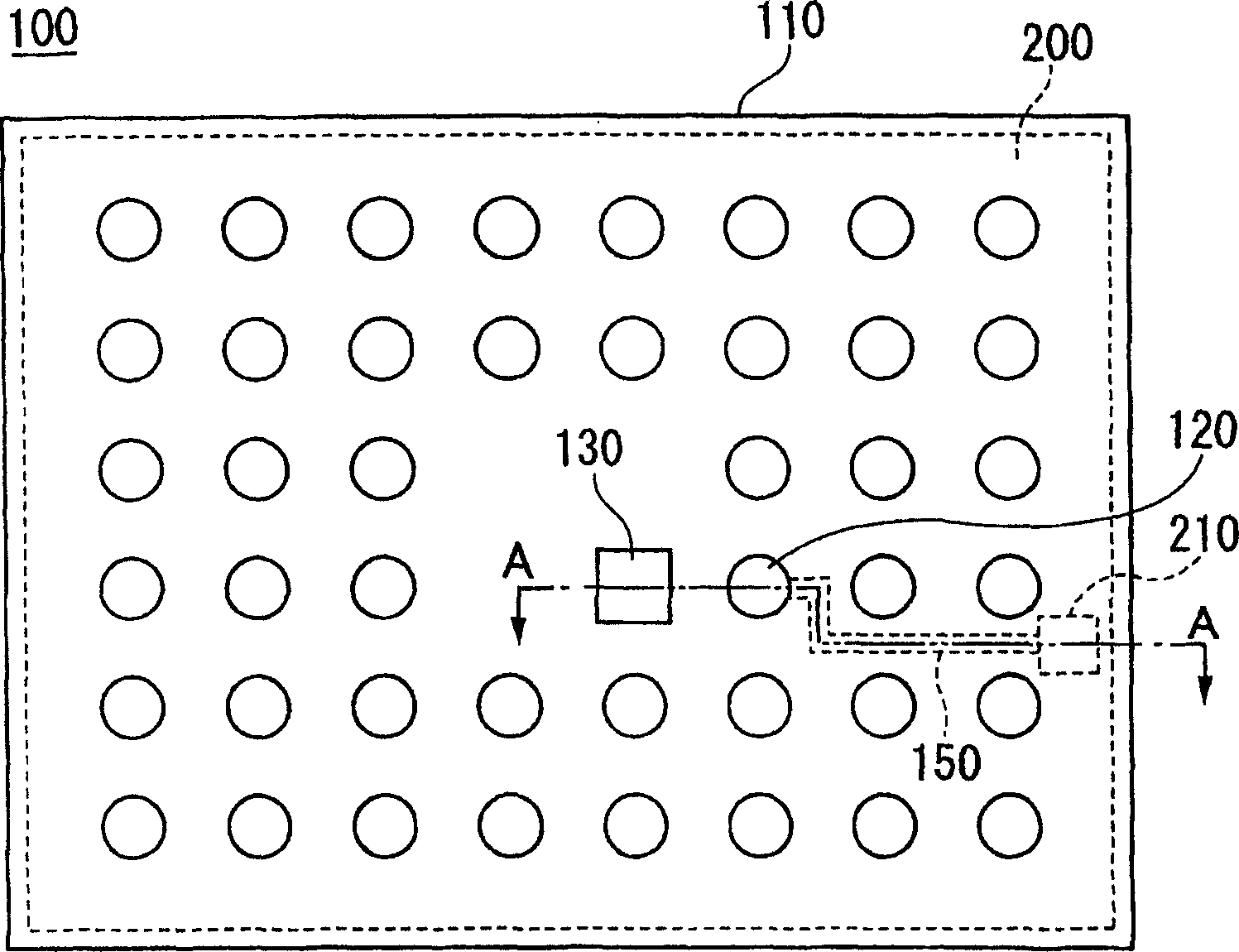
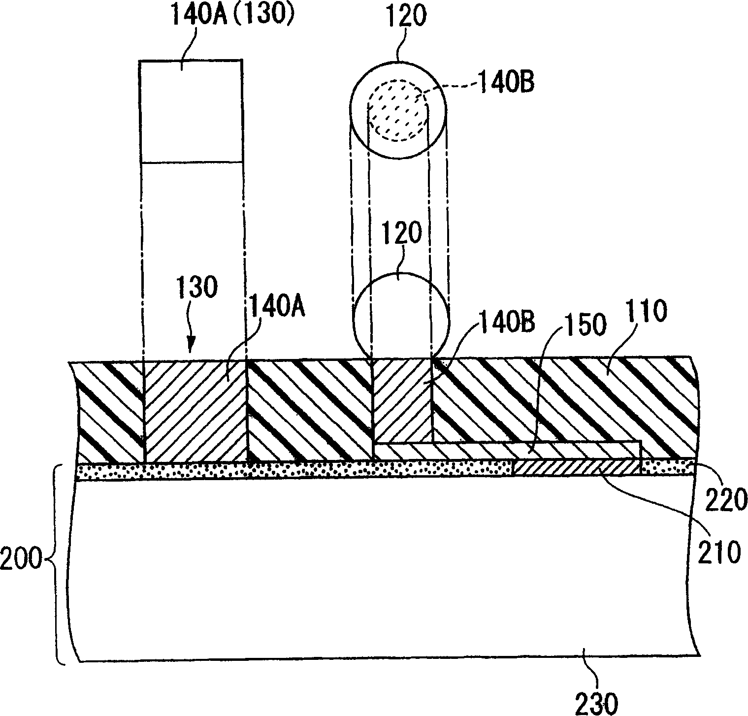
[0026] figure 1 The appearance of a predetermined surface (or back surface) of the chip-scale package 100 according to the first embodiment of the present invention is shown. Here, the chip size package 100 may correspond to a surface mount chip package, and it may independently hold two hundred "square" semiconductor chips 200 therein. Each individual semiconductor chip 200 has an integrated circuit (not shown) formed on its main surface, and is covered with a molding resin (or molding resin) forming the package case 110 . Incidentally, the molding resin is formed so as to avoid a copper post used as a mark, which will be described below. That is, copper posts used as markers and other copper posts used as conductors are embedded in molding resin.
[0027] The solder balls 120 constituting the external electrodes are formed on one surface of the package 110 matching the main surface of the semiconductor chip 200 (in other words, the outer surface of the package case 100 co...
no. 2 example
[0041] In the first embodiment, the polished surface of the copper post 140A is directly used for the marker 130, whereby the copper post 140A is exposed to the outside atmosphere and will be easily damaged due to oxidation, which will affect the reliability of manufacturing. In order to avoid this drawback, the second embodiment such as Figure 5 Constructed as shown, a solder layer 160 is formed again on the polished surface of the copper post 140A, and this solder layer is used as a discrimination element of the marker 130 .
[0042] As above, the size of the copper post 140A is larger than that of the copper post 140B, whereby the square cross-sectional area of the copper post 140A becomes larger than the circular cross-sectional area of the copper post 140B. The solder layer 160 is made of the same material as the solder ball 120 serving as an external electrode, wherein the material is heat-treated to form the solder layer 160 in a predetermined shape and size. As d...
PUM
 Abstract
Description
Claims
Application Information
 - R&D Engineer
- R&D Manager
- IP Professional
- Industry Leading Data Capabilities
- Powerful AI technology
- Patent DNA Extraction
Browse by: Latest US Patents, China's latest patents, Technical Efficacy Thesaurus, Application Domain, Technology Topic, Popular Technical Reports.
© 2024 PatSnap. All rights reserved.Legal|Privacy policy|Modern Slavery Act Transparency Statement|Sitemap|About US| Contact US: help@patsnap.com