Semiconductor laser and method for manufacturing same
A manufacturing method, semiconductor technology, applied in the direction of semiconductor lasers, lasers, laser components, etc., can solve problems such as the inability to prevent sequential tapers, the difficulty in forming vertical ridge sides, and the difficulty in ensuring that the corrosion stop layer stops corrosion, etc. , to achieve high output
- Summary
- Abstract
- Description
- Claims
- Application Information
AI Technical Summary
Problems solved by technology
Method used
Image
Examples
no. 1 example
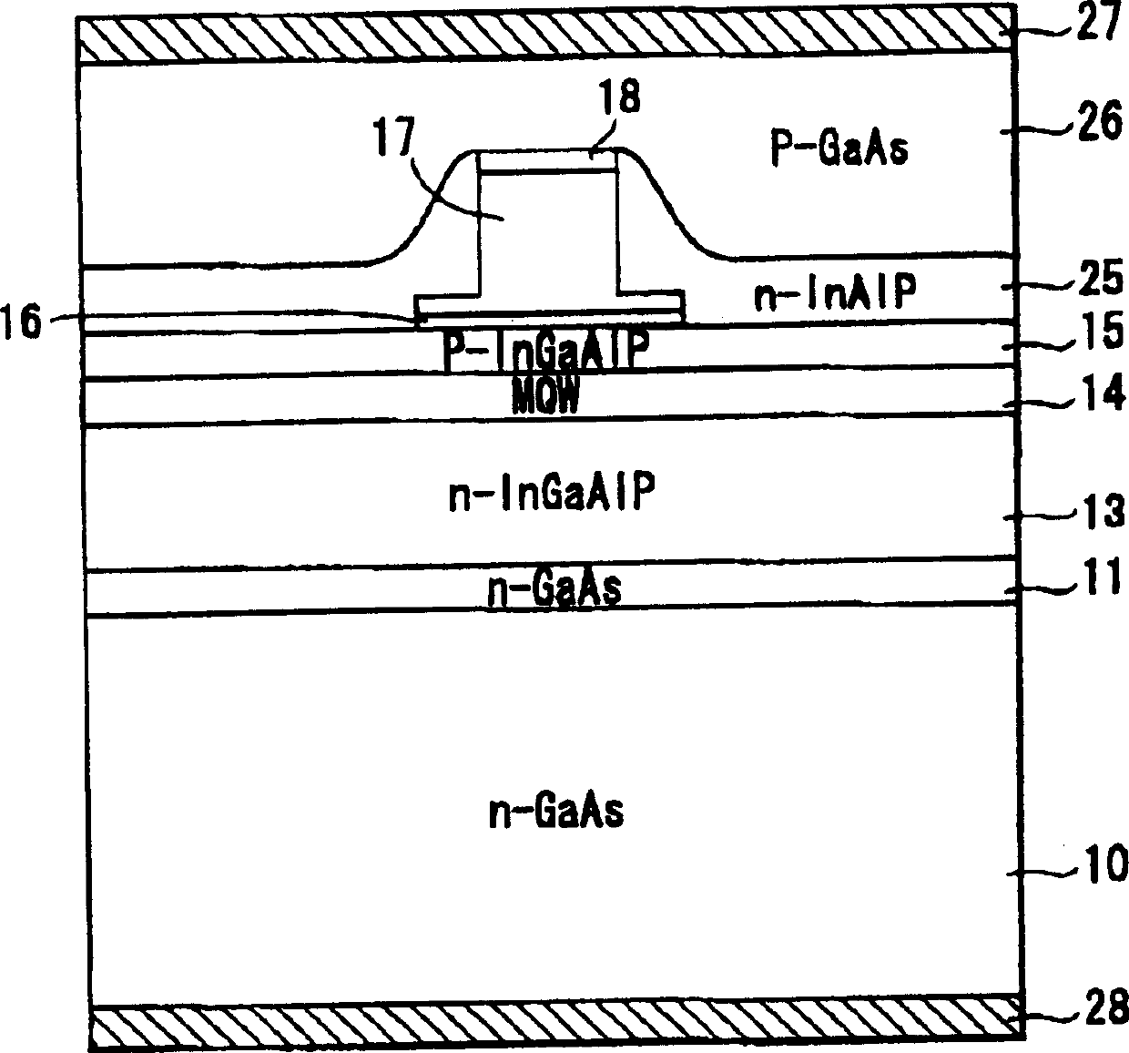
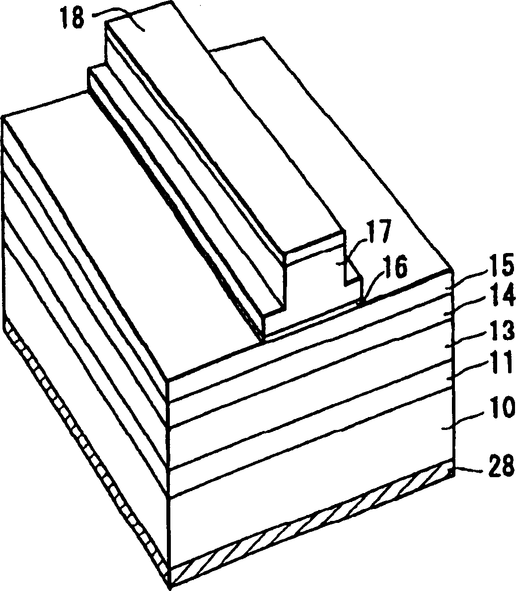
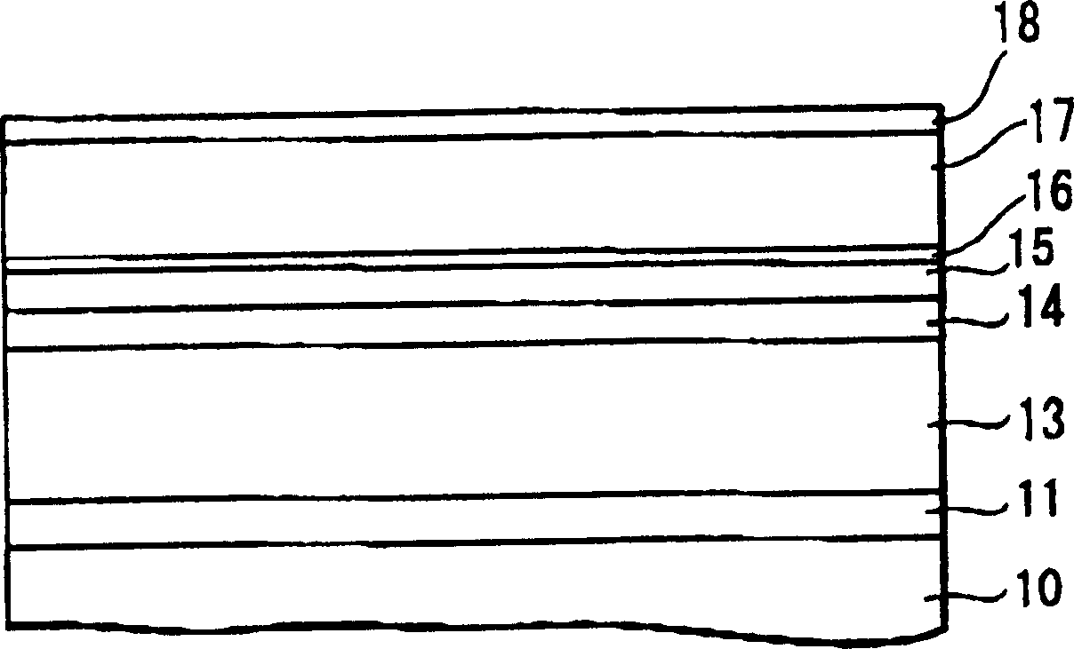
[0038] The structure of a red semiconductor laser according to a first embodiment of the present invention is shown in FIGS. 1A and 1B. The n-type GaAs buffer layer 11 , the n-type InGaAlP cladding layer 13 , the MQW active layer 4 composed of undoped InGaAlP / InGaP, and the p-type InGaAlP cladding layer 15 are formed on the n-type GaAs substrate 10 . As shown in FIG. 1B , a striped ridge is formed on the p-type InGaAlP cladding layer 15 , and the striped ridge is composed of a p-type InGaP etch stop layer 16 , a p-type InGaAlP cladding layer 17 and a p-type InGaP capping layer 18 .
[0039] The ridge functions as a current gathering part, and its sides are treated substantially vertically. In addition, the bottom of the p cladding layer 17 and the etch stop layer 16 have a wider width than any other region. The sides of the ridge may embed an n-type InAlP barrier layer 25, and a p-type GaAs contact layer 26 is formed on the capping layer 18 of the ridge and planarizes the bar...
no. 2 example
[0058] In the red semiconductor laser according to the second embodiment of the present invention, the blocking layer 45 is made of SiO 2 form, as shown in Figure 4.
[0059] An n-type GaAs buffer layer 31, an n-type InGaAlP cladding layer 33, an MQW active layer 34 composed of undoped InGaAlP / InGaP, and a p-type InGaAlP cladding layer 35 are formed on an n-type GaAs substrate 30. A strip-shaped ridge composed of the etch stop layer 36 , the p-type InGaAlP cladding layer 37 , the p-type InGaP capping layer 38 and the p-type GaAs contact layer 46 is formed thereon.
[0060] The sides of the ridge are processed substantially vertically, and the bottom of the p cladding layer 37 and the etch stop layer 36 have a wider width than any other region. The sides of the ridge can be embedded with SiO 2 film (barrier layer) 45, and planarize the surface. In addition, a p-side electrode 47 is formed on the ridge of the contact layer 46 and the SiO 2 On the film 45 , an n-side electrod...
PUM
 Abstract
Description
Claims
Application Information
 - R&D
- Intellectual Property
- Life Sciences
- Materials
- Tech Scout
- Unparalleled Data Quality
- Higher Quality Content
- 60% Fewer Hallucinations
Browse by: Latest US Patents, China's latest patents, Technical Efficacy Thesaurus, Application Domain, Technology Topic, Popular Technical Reports.
© 2025 PatSnap. All rights reserved.Legal|Privacy policy|Modern Slavery Act Transparency Statement|Sitemap|About US| Contact US: help@patsnap.com


